Keywords
|
| ultra wideband antenna; planar patch antenna; compact; group delay |
INTRODUCTION
|
| In the recent years, an enormous need for wireless communications due to the great wireless lifestyle benefits. Because the wireless communications services claims, a continuous dramatic increase in the market of wireless systems. Latest wireless systems are striving to offer a wide range of different applications such as data and video to maximum number of mobile users with high data rates. Though, these systems are limited due to the shortage of resources such as frequency spectrum and power. Therefore, new technologies that are able to overcome these limits are needed [1]. |
| Nowadays, the technology of ultra wide bandwidth is a potential methodology to many wireless communication systems. The history of ultra wideband is built on the concept of impulse radio because very high data rates have been transmitted using energy pulses rather than a narrowband frequency carrier [2]. Most of the latest research in this area is focused on optimizing the antenna performance while maintaining the structure size as small as possible. However, some designs characteristics such gain and wide operating frequency have been degradeddue toreducing their physical sizes. Thus, it is a challenging issue and motivating for researchersto preserve both size and performance for an UWB antenna [3-6]. |
| Based on the rules of Federal Communications Commission (FCC), Ultra wide band is any system that has a bandwidth of 500 MHZ or more or a system that have fractional bandwidth larger than or equal to 0.2 [7,8]. The formula below defines fractional bandwidth: |
| Fractional BW= 2x(fh-fL)/(fh+fl) |
| Where: fh and fL are the upper limit and the lower limits of the frequency operation |
| Also, in 2002 federal communications commission (FCC) stated a new regulation for the technology of ultra wide band (UWB) by releasing an unlicensed wide frequency band. It is from 3.1 GHz to 10.6 GHz, which is a bandwidth of 7.5 GHz [9,10]. |
| Ultra Wide Band Antennas have several great advantages that make them attractive and interesting technology over the recent years. They provide extremely high data rates and capacity with low power consumption [8]. In addition, they operate over a wide frequency spectrum, which make them useful for many applications [11]. The maximum limit of data rate or the ideal capacity is controlled by two main factors. These influences are the channel bandwidth and the signal to noise ratio. Based on Shannon’s formula, by maximizing the channel bandwidth (B), the system data rate (R or C) increases [12]. From this key principle ultra wide band (UWB) systems support extremely high data rates. |
| C = B log2 (l+S/N) |
| Where: |
| C: the maximum system capacity measured in bits per seconds |
| B: the channel bandwidth in Hz |
| S/N: signal to noise ratio, which is unitless watt/watt |
STRUCTURE DESIGN
|
| The configuration of the designed antenna is shown in figure 1 and it is labeled with the parameters. The used feeding technique is coplanar waveguide (CPW) as illustrated below with 50 ohms characteristics impedance. In general, CPW feeding method is more beneficial than many other feeding techniques such as probe or microstrip line [13]. It makes the antenna more appropriate for most of compact wireless devices due simplicity in fabrication, and one planar structure [14]. The antenna fed using CPW provides mutual coupling between the structure adjacent lines [15, 16]. |
| The designed transmission feeding line is 8 mm long and 1 mm wide. The printed patch antennas are very attractive in ultra wideband UWB systems due to the excellent virtues of light in weight, low cost, and easy in fabrication [17]. Thus, the proposed antenna, which is made of copper material, is printed on a substrate of FR4 material with permittivity of εr=4.3 and los tangent of 0.025. The substrate has a thickness of 2.4 mm, length of 24 mm, and 23 mm width. The CPW is feeding the radiating parts, which are composed of one main octagonal element partially containing three small octagonal elements. The main element has a radius of 4 mm and each of the other small octagonal parts hasa radius of 2 mm. Different views of the designed ultra wideband (UWB) antenna are demonstrated in the figures below. Different iterations of the structure widths and heights have been studied to optimize the performance. After optimizing the structure results, the design parameters are shown in table 1. The simulations results and experimental measurements are shown and discussed in the following section. |
SIMULATION RESULTS AND ANALYSIS
|
| Since a microstrip antenna typically has only one resonant frequency, its bandwidth is not a wide band generally. Therefore, having multiple overlapped resonant frequencies usually leads to an ultra wide band (UWB). Most of ultra wide band antennasare based on this principle [6]. |
| The structure design has been simulated using CST microwave studio simulation software. The antenna performance demonstrates that it has extremely wide frequency band (from about 2.9 to more than 18 GHZ), which makes the design appropriate especially for ultra wideband applications. Thus, the designed antenna results show good impedance matching over its wide bandwidth. The excellent impedance matching translates to high antenna efficiency and power transfer [18]. Figure 4 reveals the return loss (S11) plots in dB for different feeding line width (wf) values where the optimum value occurs to be at wf=1 mm. It has been noticed that as the feeding width increases the impedance matching decreases and the power transfer downgrades as well. Thus, the shortage in S11 values will lower the ultra wide bandwidth based on -10 dB criteria, which shows the delivered power amount to the antenna. Also, for optimization purposes, the design has been simulated with different radiuses of the main octagonal radiating element. These radiuses are 3.5 mm, 4 mm, 4.5 mm, and 5 mm and the simulation return loss in dB plots are shown in figure 5. The graphs show similarity between the four situations in terms of resonant frequencies. However, the plot of r=4 mm has the best return loss values (S11) over the widespread bandwidth. Moreover, it has been found that best substrate material for this design that provides the prime simulation results is FR4 material withïÿýïÿýr=4.3. The FR4 substrate makes the operating frequency wider and maximizes the impedance matching, and the gain values in this design. Also, FR4 dielectric material is easily found and low cost in manufacturing companies. Different substrate materials such as Duroid RT 5880, and Duroid RT 6006 have been tested as illustrated in figure 6. In terms of the voltage standing wave ratio, the plot of VSWR with respect to frequency is shown in figure 8 and the bandwidth is the frequency range over which VSWR<2. |
| The maximum limit of power emission for UWB communication systems devices is set by FCC to be -41.3 dBm/MHz and the limits are set to be very low in order to prevent UWB applications from introducing interference to other wireless applications [7]. This design, which has excellent gain values, can reach the EIRP value with low input power. The Effective isotropic radiated power (EIRP) is expressed as below: |
| EIRP=PTXGTX |
| Where: PTX is the transmitted power and GTX is the maximum gain value [18] |
| Thus, according to the previous equation, the proposed UWB antenna, which has excellent gain values, keeps battery life longer which is an essential improvement for wireless communication devices. The normalized radiation pattern of the designed antenna in E and H planes for different frequencies in the operating wide bandwidth (3.48 GHz, 4 GHz, and 6.64 GHz) are shown in figure 9 from simulation and fabrication measurements. The E plane has an excellent radiation shape of doughnut for the threeresonant frequencies. Regarding H plane, the radiation pattern is clearly Omni-directional during the entire bandwidth as illustrated in the figure. Thus, the proposed patch is appropriate for ultra wideband systems. Also, the simulated and measured antenna gain over the UWB are plotted in figure 10, which shows excellent values with average more than 5 dB. Both results, simulation and experimental measurements, show very good agreements with small differences due to the fabrication tolerance and SMA connector soldering. |
| It is important to confirm that no distortion happened to the signal while transmitting for UWB antennas during their wide bandwidth. Group delay is very helpful parameter can be calculated in order to give an indication that no distortion occurred. It can be calculated from the phase of S21 where two identical antennas are placed face-to-face, face to side, and side to side inside anechoic chamber [19]. |
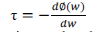 |
| A linear phase is translated to a constant group delay whereas the deviations of the phase represent variations in the group delay time. The average transit time through two antennas or ports systems is characterized by the average group delay [20]. Thus, an excellent UWB antenna should have stable group delay through the operating frequency. Rapid changes or spikes in the group delay signal might cause a distortion in the transmitted signal which could lead to inter-symbol interference (ISI). Usually, group delay in the range of few nanoseconds or less and small variations are very normal and acceptable. |
| The group delay of this designed antenna has been calculated using the previous equation from the phase of the S21. For all the three situations, which are face-to-face, side-to-side, and face-to-side. The presented ultra wideband antenna shows almost stable delay time of less than 1 nanosecond with small variations during the UWB. The figures below (11, 12, and 13) demonstrate the group delay versus frequency.Finally, the main results for different frequencies are summarized in the table 2. |
CONCLUSION AND FUTURE WORK
|
| In this paper, a new ultra wideband (UWB) antenna has been designed, simulated and fabricated. The structure is simple in design, easy in fabrication, and low in cost. The results for both simulation and fabrication show excellent performance in terms of matching between the antenna parts and feeding line. Also, the designed antenna has extremely wide bandwidth that makes it adequate for UWB wireless communications applications. Furthermore, the simulation results of the proposed antenna have excellent gain values over the wide operating frequency that will have positive consequence on the battery life of the wireless system. |
Tables at a glance
|
 |
|
| Table 1 |
Table 2 |
|
| |
Figures at a glance
|
 |
 |
 |
 |
 |
| Figure 1 |
Figure 2 |
Figure 3 |
Figure 4 |
Figure 5 |
|
 |
 |
 |
 |
| Figure 6 |
Figure 7 |
Figure 8 |
Figure 9 |
|
 |
 |
 |
 |
| Figure 10 |
Figure 11 |
Figure 12 |
Figure 13 |
|
| |
References
|
- Arslan, H.; Chen, Z. & Benedetto, M., ”Ultra Wideband Wireless Communication," John Wiley & Sons, Inc., 0471715212, New Jersey, 2006.
- J. Liang, “Antenna Study and Design for Ultra Wideband Communication Applications,” PhD Thesis, University of London, United Kingdom,July 2006.
- M. Sarifi, S. Podilchak, M. Essaaidi, and Y. Antar, “Compact Disc Monopole Antennas for Current and Future Ultrawideband (UWB)
- D. Chen and C. Cheng, “A Novel Compact Ultra-Wideband (UWB) Wide Slot Antenna with Via Holes,” Progress in ElectromagneticsResearch, vol. 94, pp. 343-349, 2009.
- R. Azim, M. Islam, and N. Misran, “Compact Tapered-Shape Slot Antennafor UWB Applications,” IEEE Antennas and WirelessPropagation Letters, vol. 10, pp. 1190-1193, 2011.
- Gautam, S. Yadav, and B. Kanaujia, “A CPW-Fed Compact UWB Microstrip Antenna,” IEEE Antennas and Wireless PropagationLetters, vol. 12, pp. 151-154, 2013.
- Mohsen Koohestani, J.-F. Zürcher, Antonio A. Moreira, and Anja K. Skrivervik,” A Novel, Low-Profile, Vertically-Polarized UWB Antenna for WBAN,” IEEE Transactions On Antennas And Propagation, Vol. 62, No. 4, April 2014.
- Federal Communication Commission, “First Report and Order, Revision of Part15 of the Commission's Rules Regarding Ultra-Wideband TransmissionSystem,” FCC 02 48, 2002.
- D. Wentzloff, R. Blazquez, F. Lee, B. Ginsburg, J. Powell and A. Chandrakasan, “System Design Considerations for Ultra-Wideband Communication," IEEE Communications magazine, vol. 43, pp.114-121, August 2005.
- Malay Yadav,” Coplanar Waveguide Fed UWB Antenna with Dual Band Notch Characteristics,” Master Thesis, Thapar University, June 2012.
- Oppermann, M. Hamalainen and J. Iinatti, "UWB Theory and Applications"John Wiley & Sons, Ltd, 2004.
- H. Oraizi and S. Hedayati, “Miniaturized UWB monopole microstrip antenna design by the combination of GiusepePeano and Sierpinski carpet fractals,” IEEE Antennas Wireless Propag. Lett., vol. 10, pp. 67–70, 2011.
- Mobashsher, A.T., Bais, B., Misran, N., Islam, M.T., “Compact Wideband Microstrip Antenna For Universal 5 Ghz WLAN Applications,” Australian Journal of Basic and Applied Sciences, 4 (8), 3411-3417, 2010.
- Deepti Das Krishna,” Investigations On Broadband Planar MonopoleAnd Slot Radiators And Their Suitability For UWB Applications,” Phd Thesis, Cochin University Of Science And Technology Cochin-682022, India, September 2010.
- Qing, X., Chen, Z.N.,“Compact coplanar waveguide-fed ultra-wideband monopole-like slot antenna,” IET Microwaves, Antennas &Propagation, 3(5), 889-898, 2009.
- Mobashsher, A.T., Islam, M.T., Misran, N.,“Wideband compact antenna with partially radiating coplanar ground plane,” The Applied Computational Electromagnetics Society Journal, 26 (1), 73-81, 2010.
- Z. Chen, T. See and X. Qing, "Small Printed Ultra Wideband Antenna withReduced Ground Plane Effect," IEEE Transactions on Antennas andPropagation, vol. 55, pp. 383-388, February 2007.
- Hans Schantz, The Art and Science of Ultrawideband Antennas,Artech House, Boston, Mass, USA, 2005.
- Gabriela Quintero Diaz De Leon, “Analysis and Design of Ultra-Wideband Antennas in the Spectral and Temporal Domains,” PhD Thesis, EcolePolytechniqueFederale De Lausanne, 2010.
- Understanding the Fundamental Principles of Vector Network Analysis, Application note 1287-1 ed., Agilnet Technologies, 2005.
|