Research & Reviews: Journal of Material Sciences
ISSN:2321-6212
ISSN:2321-6212
1Micro/Nano Technology Center, Tokai University, 4-1-1 Kitakaname, Hiratsuka-city, Kanagawa 259-1292, Japan
2Institute of Innovative Science and Technology, Tokai University, 4-1-1 Kitakaname, Hiratsuka-city, Kanagawa 259-1292, Japan
3School of Chemistry and Chemical Engineering, Key Laboratory for Thin Film and Microfabrication of the Ministry of Education, Shanghai Jiao Tong University, Shanghai 200240, China
4School of Mechanical Engineering, University of Science and Technology Beijing, No. 30 Xueyuan Road, Haidian District, 100083, China
#Contributed equally to this work
Received Date: 09/05/2017; Accepted Date: 03/10/2017; Published Date: 10/10/2017
DOI: 10.4172/2321-6212.1000195
Visit for more related articles at Research & Reviews: Journal of Material Sciences
Super elliptical plates which are defined by shapes between an ellipse and a rectangle have a wide range of use in engineering applications. Investigations on non-linear behaviors of super elliptical isotropic plates are available in the literature, while investigations on nonlinear behaviors of FGM super elliptical plates haven’t been reported at present. In this paper, nonlinear bending and thermal post-buckling analysis are first presented for functionally graded super elliptical plates based on classical plate theory. Material properties are assumed to be temperature-dependent and graded in the thickness direction. The numerical illustrations concern the nonlinear behaviors of functional graded plates with immovable simply supported edge and immovable clamped edge. Influences played by different supported boundaries, thermal environmental conditions, and volume fraction index are discussed in detail using Ritz method
Microfabrication and nanofabrication are revolutionary milestones in fabrication technologies, many enlightening methods have been introduced e.g., micro-EDM [1], micro incremental forming [2], microlithography [3], nano-imprinting [4] etc. Microfabrication is also been recognized as micromanufacturing in term of describing the process for fabricating miniature structures. Historically, fabrication of integrated circuit and semiconductor devices are the first application for microtechnology. With the advances in microelectromechanical systems (MEMS) and other nanotechnology, application of microfabrication has been greatly extended. As the matter of fact, more development and research has been carried out, and all of them require accurate pattern examine with precise define in dimensions and geometries. Therefore, pattern examine methods are in demand.
Since EBL (Electron Beam Lithography) has become the essential fabrication method for production and research, therefore, EBL is used for pattern generation in this paper. In order to analyze the generated patterns accurately, various examine methods are used as comparison. The objective of this paper is to compare sequential light, scanning electron and atomic force pattern examine methods of advantages, disadvantages and limitations upon micro-scale square cuboid patterns.
EBL (Electron Beam Lithography) is a high resolution microlithography method by scanning a beam of electrons to remove non-exposed or exposed spot of the resist-covered material. It has been consolidated as the most important micronanofabrication technique for patterning from 10 nm to 10 mm [5], the most flexible method that can undertake the fabrication of submicron structures with complex geometries, and main production of photomask for other photolithographic techniques. All these characters made EBL one of the dominant techniques in micro- and nanofabrication.
The 4-inch silicon wafer with thickness of 525 μm, shown as Figure 1, is used as the material, and the procedure for pattern generating is operated in a super clean room. EBL (Electron Beam lithography) method is used for pattern generating. The overall process includes:

Figure 1: (a) 4-Inch Silicon Wafer Sample; (b) Electron-beam lithography machine (Model: F5112+VD01, ADVANTEST).
Step 1
Resist Coating, the Electron Beam resist (OEBR-CAP112PM) is applied by method known as spin coating. The wafer is spun rapidly by a spin coater (Model: SC-400) at 3000 rpm for 60 seconds while being coated with the resist.
Step 2
Pre-bake, heating the silicon wafer at 110°C for three minutes by a lab Oven (Model: DNF-44). The purpose of the pre-bake is to evaporate the excess coating solvent and harden the resist.
Step 3
Exposure, using Electron Beam Lithography Machine (Model: EB Writer F5112+VD01, ADVANTEST), as shown in Figure 1b, to scan a beam of electrons across resist surface to remove exposed spot of the resist-covered material and create desired pattern structure.
Step 4
Development, in this stage, an ammonium tetramethyl hydroxide aqueous solution (2.38%, ZTMA-100) is applied to the wafer for 60 seconds.
Step 5
Post-Baking, heating the wafer at 110°C for three minutes. The purpose of the post-bake is to stabilize and harden the resist while removing traces of development chemicals.
Step 6
Etching, using SF6 (sulfur hexafluoride) with CHF3 (Trifluoromethane) plasma RIE (Reactive Ion Etching) machine (Model: CE-300I, ULVAC) to etch the silicon wafer.
Sequential Light Examine Method
First, the generated patterns (Table 1) from EBL method have been investigated by a compound optical microscope (Model: VH-Z100, Keyence) with CCD (Charge-Coupled Device) monitor (Model: VHX-200/100F, Keyence) which uses visible light with a system of lenses to magnify images of small objects. In the optical microscope, the specimen for observation is assumed to be a light absorbing object, in this way, the light from the microscope condenser through the specimen will not be deviated. Such light is recognized as direct light or undeviated light. Some of the light, partially deviated when it encounters specimen parts, is recognized as diffracted light. Once multiple lenses collect both direct light and diffracted light from the specimen, then a separate set of lenses is used to focus the light into image. The maximum magnification is limited to 1000x. The governing equation of resolution as below:
 (1)
(1)
where d is the resolution, λ is the wavelength of light, NA is the numerical aperture of the objective lens. In most cases, λ is assumed to be 550 nm (green light), and air is used as medium with highest NA of 0.95, therefore, the lowest value of resolution is about 300 nm from the equation of resolution.
After examine the pattern #1 (Table 1), a 10 μm x 10 μm square cuboid pattern, the image caught by CCD camera, as shown in Figure 2a, reveals a real-time vivid image at maximum magnification (1000X). The pattern is neatly formed in square geometric shape. The dimension of the square is 10.08 μm x 10.08 μm measured from the CCD micrograph. However, the depth of the pattern is vague for visual investigation or precise measurement.

Figure 2: CCD images of (a) pattern #1 and (b) pattern #2.
Table 1. Parameters of samples.
| Pattern # | Geometry | Area (µm) | Depth (µm) |
|---|---|---|---|
| 1 | Square Cuboid | 10 x 10 | 1 |
| 2 | Square Cuboid | 2.5 x 2.5 | 1 |
In order to explore the size limitation of a compound optical microscope, pattern #2 (Table 1), a 2.5 μm x 2.5 μm square cuboid pattern, is examined in the same setting (maximum magnification, 0° tilt angle). As shown in Figure 2b, the image is vivid, however, the pattern appears to be difficult for accurate measurement, and resolution limit is reached. Theoretically, the lowest value of resolution can be reached at 300 nm, but in practical, when the pattern length is close to or lower than 1 μm, the quality and magnification of micrograph starts to degrade. Hence, the compound optical microscope is not suitable for submicron pattern examine.
Atomic Force Examine Method
Atomic Force Examine Method was introduced by Bining, et al. [6]. Same year, a working prototype AFM (Atomic Force Microscopy) is invented. Today, AFM is considered as a versatile technique for imaging surface topography of specimen with very high-resolution up to nanometer scale. AFM consists of a cantilever with a probe for scanning the surface, and a laser spot is used for measuring the deflection from the tip of the cantilever. The deflection of the cantilever is expressed by:
 (2)
(2)
 (3)
(3)
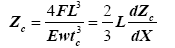
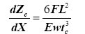
Where E is the Young’s modulus of the cantilever material; F is the force applied to the end of the cantilever in normal direction; L, w and tc is the length, width and thickness of the cantilever correspondingly; dZc/dX is the change of the endslope.
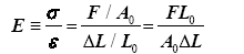
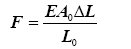
The Young’s Modulus is expressed by
 (4)
(4)
 (5)
(5)
Where E is the modulus of elasticity; σ is then tensile stress; ε is the tensile strain; F is the force applied to the object; A0 is the original cross-sectional area through which the force is applied; ΔL is the amount by which the length of the object changes; L0 is the original length of the object.
The expression for cantilever’s spring constant is:
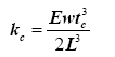 (6)
(6)
More accurate expression for cantilever’s spring constant is optimized by Sader [7]:
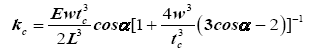 (7)
(7)
Where α is an opening angle.
In this section, pattern #2 (Table 1) is been examined by AFM (Model: NanoNaviIIe, SII). The whole examine procedure is about 20 minutes which includes Initial – Preparation – Parameter – Approach – Scan.
In the preparation step, as shown in Figure 3 , it is important to adjust the laser beam to the cantilever and the laser spot into the frame at center of the laser position dialog.

Figure 3: AFM Set-up; (a) Schematic of AFM, (b) Laser Adjustment, (c) Laser Spot on Cantilever.
After the scanning, AFM images, as shown in Figure 4a and 4b generate a colorful three-dimensional structure and detailed analysis in very precise measurement of the specimen e.g., Ra, Rp, RMS and Rz (Table 2). Ra is the surface roughness average. Rp is the maximum profile peak height. RMS is the root mean square average of the profile heights over the evaluation length. Rz is the average maximum height of the profile. However, the scanning area of the specimen is limited approximately to 150 μm x 150 μm with the maximum height or depth in terms of 10-20 μm. Furthermore, the corner sides of the specimen are unclearly formed due to the defect of AFM tapping mode.

Figure 4: AFM micrograph of Pattern #2; (a) depth measure; (b) 3D image.
Table 2. Measurement parameters.
| Measurements | Ra (nm) | Rp (nm) | RMS(nm) | Rz (nm) |
|---|---|---|---|---|
| 1.16E+02 | 2.25E+02 | 1.94E+02 | 1.12E+03 |
Table 3. Overall Comparison among sequential light, AFM and SEM.
Scanning Electron Examine Method
In this section, a SEM (Scanning Electron Microscope) is used for pattern examine. The method is to make the electrons interact with atoms of the specimen in order to receive signals that contain specimen’s surface topography. As shown in Figure 5a, a typical SEM uses an electron gun to generate an electron beam thermionically with a tungsten filament cathode. SEM itself has condenser and objective lenses, and functionalities are to focus electron beam to a spot not for image purpose like optical microscope. The energy range for the electron beam is from 0.5 keV to 40 keV. The examined specimen interacts with the electron beam, which causes electron beam to lose energy by scattering and absorption. Therefore, images can be generated by the specimen current distribution which is detected from the beam current absorption by the specimen.

Figure 5: Scanning Electron Microscope; (a) diagram of Scanning Electron Microscope; (b) SEM (Model: FE-SEM S-4700, Hitachi); (c) SEM Micrograph of Pattern #2.
The eight Maxwell’s equations which written in modern vector notation [8], as the main formulas for electromagnetic field generated by the magnetic lenses, are expressed as follows:
The law of total currents:
 (8)
(8)
The equation of magnetic force:
μH = ∇ ×A (9)
Ampere’s circuital law:
∇ × H = Jtot (10)
Electromotive force created by convection, induction, and by static electricity:
 (11)
(11)
The electric elasticity equation:
 (12)
(12)
Ohm’s law:
 (13)
(13)
Gauss’s law:
∇⋅ D = ρ (14)
Equation of continuity:
 (15)
(15)
Where H is the magnetizing field; J is the current density; D is the displacement field, ρ is the free charge density, A is the magnetic potential, E is the electromotive force; φ is the electric potential; σ is the electrical conductivity.
A SEM micrograph is in three-dimensional appearance and useful for surface structure study. The magnification of SEM ranges from 10X to more than 500,000X which is more than 500 times the magnification limit of the compound optical microscope (refer to Section 3.1).
The pattern #2 (Table 1) is scanned at 30° tilt angle with a high energy beam of electrons by SEM (Model: FE-SEM S-4700, Hitachi), as shown in Figure 5b, in a clean room environment. The energy of electron beam is 10 keV which is a typical value for high-vacuum SEM examination. Figure 5c shows that SEM is able to provide real-time black-and-white vivid image of the pattern. Although, the structure is revealed in medium resolution quality compared to AFM, the scanning area of the specimen and scanning rate is superior to AFM. The same pattern has been examined by a compound optical microscope (Model: VH-Z100, Keyence) (refer to Section 3.1), with comparison, it is clear that SEM is able to investigate patterns in submicron [9].
Table 3 reveals the concise comparison in the function of special treatment, scanning rate, resolution, magnification, analysis and scanning area.
| Category | Sequential Light | AFM | SEM |
|---|---|---|---|
| Special Treatment | No | No | Vacuum |
| Scanning Rate | High | Very low | Medium |
| Resolution | Medium | High | High |
| Magnification | Low | Very High | High |
| Analysis | Medium | High | Low |
| Scanning Area | Medium | Limited | High |
| Depth | Medium | High | High |
| Surface Roughness | Medium | High | High |
In this study, patterns (Table 1) are generated by EBL (Electron Beam Lithography), and examined by three different imaging methods: Sequential Light, Atomic Force and Scanning Electron. In order to distinguish functionalities of these methods, a compound optical microscope (Model: VH-Z100, Keyence) with CCD (Charge-Coupled Device) monitor (Model: VHX-200/100F, Keyence), an AFM (Atomic Force Microscopy) (Model: NanoNaviIIe, SII) and a SEM (Scanning Electron Microscopy) (Model: FE-SEM S-4700, Hitachi) is operated as pattern examine apparatuses. After proper and careful investigation, characters, advantages and disadvantages of these methods are revealed.
Among three examine methods, both compound optical microscope and SEM have the advantage over AFM on scanning rate. Another major disadvantage of AFM is the area of the specimen it can examine. The scanning area of specimen by AFM is limited to approximately 150 μm x 150 μm with maximum height or depth of 10-20 μm. However, it offers much higher image resolution in comparison to the optical microscope and SEM. In contrary, the optical microscope has higher scanning rate but low magnification which is difficult to examine submicron pattern. Unlike the AFM and optical microscope, SEM has the ability to examine the pattern in a fast scanning rate with high magnification up to 500,000X. However, the major drawback is the operation environment which requires to be functioned in vacuum.
This work was supported by MEXT (Japanese Ministry of Education, Culture, Sports, Science and Technology)-Supported Program for the strategic Research Foundation at Private Universities, Grant # S1411010.