International Journal of Advanced Research in Electrical, Electronics and Instrumentation Engineering
ISSN ONLINE(2278-8875) PRINT (2320-3765)
ISSN ONLINE(2278-8875) PRINT (2320-3765)
Jayalekshmi1, Vipin Thomas1
|
| Related article at Pubmed, Scholar Google |
Visit for more related articles at International Journal of Advanced Research in Electrical, Electronics and Instrumentation Engineering
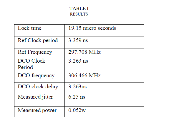
Phase Locked Loops (PLL) is a control system that generates an output signal whose phase is related to the phase of an input signal.A phase locked loop can track input frequency or it can generate a frequency that is the multiple of input frequency .PLLs are widely employed in radio,tele communications,computers etc.In order to overcome the disadvantage of analog PLLs such as the effect of leakage current and temperature, an all digital PLL is preferred here.It eliminates the problems in clocking like clock skew and jitter.The PLL is designed digitally with a divide by 4/5 prescaler in the frequency divider section.It divides the DCO frequency with two consecutive integers.The proposed method is designed in verilog and is implemented in xilinix. The major factor to be considered here is lock time.The lock time achieved here is 19.05μs
Keywords |
| Digital PLL, Prescaler, TDC,DCO, frequency divider. |
I. INTRODUCTION |
| Clock signals are particular signals which oscillates between high and low states. It changes its value from zero to one in every period. Clock signals are the heart beat of any processor. Processor executes one thing at a time and it is given by the clock. Clock signals are generated by the oscillators and all circuits in a digital system should get the clock at the same time. When the circuits get clock signals at different time, the effect may be due to clock skew.Clocking is essential for all synchronous circuits. Clock skew and jitter are the two phenomena which affects clocking.Clock skew can be caused by the static mismatches in clock path and differences in clock load. Clock jitter is the deviation in periodicity of actual clock with that of a reference clock. It is the temporal variation of the clock period. A PLL can be used to reduce these effects. It is a common part of high perfomance micro processors. PLLs are used to generate high performance micro processors in the GHZ range. |
| Traditionally, a PLL is made to function as an analog building block, but integrating an analog PLL on a digital chip is difficult. Analog PLLs are also more susceptible to noise and process variations. Digital PLLs allow a faster lock time to be achieved and are attractive for clock generation on high performance microprocessors. |
II. DIGITAL PLL |
| Digital PLL is designed by four major components. These components can be analog or digital. Analog PLL composed of PFD, charge pump, loop filter, VCO and frequency divider. The analog components such as charge pump ,loop filter and VCO are replaced in digital PLL. Charge pump and loop filter is replaced by TDC(Time to digital converter).VCO is replaced by DCO and the other two components are same in both analog and digital PLL. |
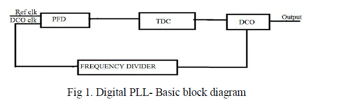 |
| The phase and frequency mismatch of reference clock and divided DCO clock are compared on PFD. The condition of ‘Lock’ is attained when Ref clock matches divided DCO clock. The PFD output is given to TDC.PFD generates up enable and down enable signals to generate the control word. The control word is generated by the thermometric decoder which controls the DCO. |
III. DESIGN OF COMPONENTS |
| A. Digital Phase Frequency Detector |
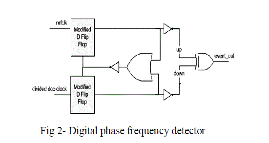
| The EXOR mechanism offers a simple yet reliable method of phase detection. One main drawback of this mechanism is its lack of sensitivity to edges. It’s a flat triggered mechanism. To eliminate this drawback the edge triggered mechanism comes into picture. The edge triggered JK mechanism is the most popular and effective one. It is sensitive to the edges and hence instantaneous corrective action can be achieved. The incoming reference signal acts as one input and the output of the Digital Controlled Oscillator (feedback of the PLL) acts as the other input. This edge triggering mechanism has been used in the design of the current ADPLL. |
| Using the above shown edge triggering mechanism a logical extension can be done by the simple D flip-flop such that it is sensitive to the edges and the clock can be eliminated. The reference signal and the output signal of the DCO are binary-valued signals. They are used to set or reset an edge triggered JK flip-flop. The time period in which the Q output of the flip-flop is a logic 1 is proportional to the phase error. |
| It compares the reference frequency and divided DCO frequency to generate the output. It consists of D flipflops, OR, XOR and NOT gates as shown in Fig 4.2. During clock, flip flop catches D input and the captured value becomes Q output until the next clock. The output of the modified D Flip-flop enters a two input NOR gate that resets the Flip-flops if both clocks are high. The up and down signals indicate if the DCO clock needs to be increased (up is true) or decreased (down is true). The event and direction signal are necessary to create the up and down enable signals for the T2D converter. |
 |
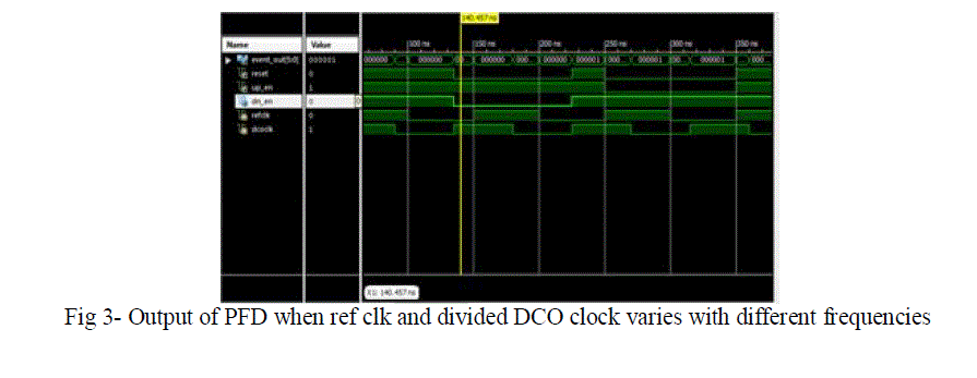 |
| If ref clk and divided DCO clock are in same phase, event_out=0 else event_out =1. |
| B. Time to Digital Converter |
| The digital loop filter is not always present in all phase locked loops. But in higher order loops where applications such as servo control, Telecommunications are involved the digital loop filter is necessary. Different Phase Detectors generate different types of signals. The simplest loop filter can be built from an Up/Down Counter. |
| TDC is used where precise time-interval measurement is required. The traditional approach to time-to-digital conversion is first to convert the time interval into a voltage. In a second step this voltage is digitized by a conventional analog-to-digital converter (ADC). The simplest technique to quantize a time interval is to count the cycles of a reference clock fitting into the respective measurement interval. |
| In earlier stages a ring oscillator type TDC is used.It is replaced by another TDC.It consists of up counter, down counter and carry ripple adder. Both counters are of 6 bit and ripple carry adder is of 7 bit. Both counters are controlled by phase detector. Initial state of up counter is 000000 and down counter is 111111. Both counters are connected to 7 bit ripple carry adder and produces the control word for the DCO |
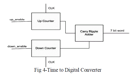 |
| An even higher resolution is achieved by subdividing one clock period asynchronously into smaller time intervals. The engine that performs this subdivision is actually what we call a digital time-to-digital converter. Hence, the resolution is the criterion that distinguishes a counter from a TDC. |
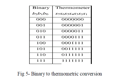
| C. Thermometric Decoder |
| Decoders are devices which do the reverse operation of encoders .Thermometric code is the one in which each digit has some pace value. It generates the control word that controls the DCO. It was obtained by modifying the general decoder to obtain the required functionality. The decoder generates a 128 bit output, of which only 126 bits are used by the DCO. These 126 bits controls the DCO. |
 |
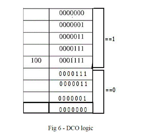
| D. Digitally Controlled Oscillator |
| DCO generates the output of the PLL.A variety of DCO designs can be used.The accumulator type DCO has been modified here as a simple logic. Also a feedback loop is provided from DCO to the PFD through frequency divider.DCO is designed to overcome the tuning stability limitation of VCO designs. The following logic is used to generate the DCO output. |
 |
 |
| E. Frequency Divider |
| It is also called clock divider. It keeps input and output phase in lock step, keeping input and output frequency same. DCO output is given to the frequency divider. The output of DCO needs to be matched to the reference frequency. When the divided frequency and reference frequency matches the PLL locks. |
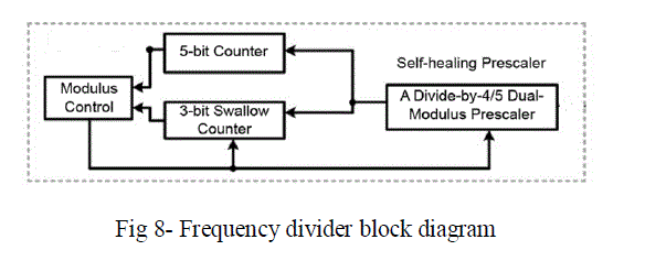 |
| The frequency divider simply divides the DCO output to matched to the reference frequency. It consists of a 5 bit counter,3 bit swallow counter ,modulus control and a divide by 4/5 dual modulus prescaler. |
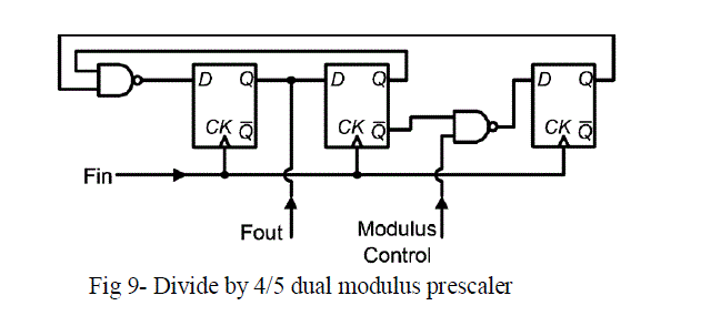
| 1) Divide by 4/5 Dual Modulus prescaler : It is also called divide by 4/5 counter. It consists of D flip flops and NOT gates. The input frequency Fin is given to all the flip flops. The selection of the counter depends on the Mode control. If MC=0,one output clock cycle is equal to 4 input clock cycles else if MC=1. One output clock cycle is equal to 5 input clock cycles. |
 |
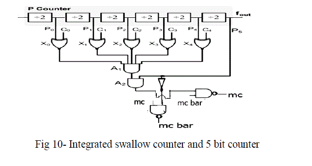
| 2) Integrated Swallow Counter and 5 bit Counter : MC is also used to control 5 bit counter and swallow counter so that it is integrated. It consists of divide by two counters, XOR,AND,NAND,NOT gates. Output of divide by two and C input is given to the XOR gates. The five XOR gate outputs are combined in AND gate and again the out is given to two NAND gates each along with MC and MC bar. |
| Fig 10 shows the diagram of Integrated swallow counter and 5 bit counter. As it is apparent, this counter consists of a divide-by-64 (P counter) that is made up of 6 divide-by-2. Digital circuit consists of XNOR gates (X0 - X4), AND gates (A0, A1). This digital section has replaced S counter in conventional ones and has the duty to control modulus bit of dual modulus prescaler. A1 gate is driven by XNOR gates (X0 - X4). Table 4.3 shows the output of XNOR block for 4 available inputs As it’s clear, XNOR gate is an equality block. When inputs of XNOR are equal (both of them are 0 or 1), output of XNOR gate is logic one. So when the value of P counter (P5P4P3P2P1P0) is equal to predefined C number (1C4C3C2C1C0), output of A1 gate becomes logic 1 (C4-C0 bits are defined by transceiver system that changes the frequency channel of PLL). In this moment dual modulus prescaler divide input frequency by 4. When P5 changes to 0, RSFF is reset and dual modulus prescaler return to divide-by-5state. For more details, assume the P counter is in ZERO condition {P5P4P3P2P1P0=000000}. As P5 is equal to 0 and dual modulus prescaler divides input frequency by 5. Suppose we want the PLL to work in 6th frequency channel and we load the number of 6 on C4-C0 {C4C3C2C1C0=00110}. Input signal is applied and P counter increases until the value of P counter reaches the predefined C {P5P4P3P2P1P0=1C4C3C2C1C0}. (For example: P5P4P3P2P1P0=100110). In this value of P counter, output of XNOR blocks and P5 are logic 1. After this time, the prescaler divide input frequency by 7 till the P counter reaches to its maximum value (111111) and next value is 000000. For the quantity of predefined C (1C4C3C2C1C0=C), prescaler divide input frequency by 8 and for rest of number (64 – C) it divides input frequency by 7. |
 |
 |
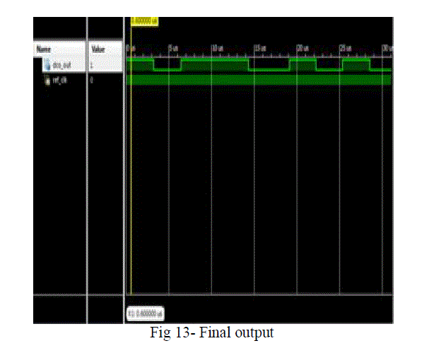
IV. FINAL SYSTEM |
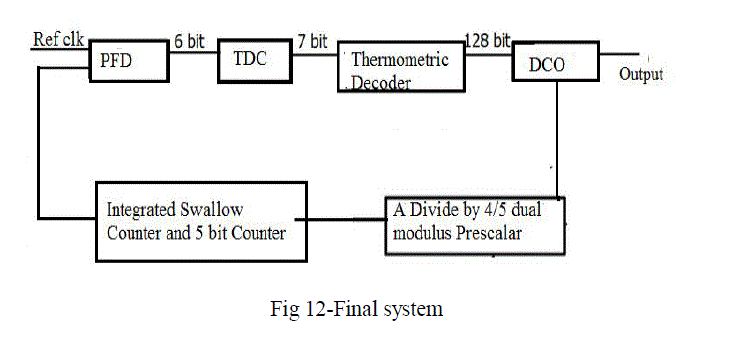
| The Fig 12 shows the proposed PLL. It consists of PFD, TDC, Thermometric Decoder, DCO, Divide by 4/5 dual modulus prescaler and integrated swallow counter and 5 bit counter. The divisional ratio is 4 to 5.The final system runs until the lock is obtained. A phase or frequency variation will cause the PLL to be activated again. |
 |
 |
V. CONCLUSION |
| A phase locked loop ensures that the clock frequencies seen at the clock inputs of various registers and flip-flops match the frequency generated by the oscillator. A divide by 4/5 dual modulus prescaler is used in the frequency divider section to obtain high resolution. The proposed PLL attains lock in 19.15 micro seconds. It has a power dissipation of 0.052 W. |
 |
References |
|