INTRODUCTION
|
| Due to rapid advancement in VLSI technology over the last two decades, aggressive scaling of memory dimensions is becoming a trend in order to achieve the minimum power requirement and higher the performance. Memories are an integral part of most of the digital devices. Reduce the power consumption of memories as well as area reduction is very important as of today to improve system performance, efficiency and reliability. |
| SRAM, the most widely used embedded memory, typically occupies the largest portion of SoC die area and often dominates the total chip power. Present day workstations low power processors, computers and super computers are using fast SRAMs and will require in the future, larger density memories with faster access time. High density low power SRAMs are needed for applications such as hand-held terminals, laptops, notebooks and IC memory cards, due to the fact that these devices frequently use battery as power source and hence it should consume power as low as possible, also it is necessary for maintaining low cooling and packing costs for these devices. The power dissipation reduction in SRAMs is not only due to power supply voltage reduction but also due to low power circuit techniques. |
| A six-transistor SRAM cell (6T SRAM cell) is conventionally used as the memory cell. However, the 6T SRAM cell produces a cell of larger size than that of a DRAM cell, resulting in a low memory density. Therefore, conventional SRAM cells that use the 6T SRAM cell have difficulty in meeting the growing demand of a larger memory capacity in mobile applications. Also the conventional six transistor (6T) SRAM cell shows poor stability at very small feature size with low power supply. During the read operation, the stability drastically decreases due to the voltage division between the access and driver transistors. |
| The SRAM cell proposed in this paper can be used to overcome these problems existing in the previous cells. We present two design techniques that reduce the power consumption of the SRAM cell. In both designs we focus on the Static Noise Margin and delay during memory operation. The rest of the paper is organized as follows. In section II we briefly review some of the SRAM memories and their operations. The proposed SRAM cells are described in section III while simulation results are discussed in section IV. Finally, section V concludes the paper. |
REVIEW OF RELATED WORKS
|
| A.8T SRAM CELL |
| 8T SRAM cell has the normal 6T SRAM design with a read decoupled path consisting of two NMOS transistors M5 & M6. Read operation of 8T SRAM is initiated by pre-charging the read bit line to full swing voltage. After pre-charging read bit line, RWL is asserted that drives access transistor M5 on. If Q=0 then M6 is on & RBL discharges through transistors M5 & M6 to ground. This decrease in the voltage of RBL is sensed by the sense amplifier. During read “1? operation, when Q=?1? M6 remains off so there will be no discharge current flow through the read path. In this situation only a very small amount of leakage current flows which is called bit line leakage. Write operation of 8T cell is similar to 6T cell but the pre-charge circuitry at the bit lines is replaced by write driver [2]. |
| This 8T-cell has 30% more area than a conventional 6T-cell.The 30% area overhead is composed of not only the two added transistors but also the contact area of the WWL, the word-line for write operations [4]. |
| B.9T SRAM cell |
| A 9T structure is proposed to improve the SNM by separating the read access structures of the original 6T cell, thus making the read SNM equal to the hold SNM. The read SNM margin is maintained by retaining the write access circuit and adding a NMOS transistor (MN9) between MN7 and MN8. As shown in Fig.2, the leakage current through MN7, MN8, and MN9 can be reduced significantly by the so-called stack effect when MN7 and MN9 are off [5]. The proposed 9T SRAM cell completely isolates the data from the bit lines during a read operation. The read staticnoise- margin of the proposed circuit is thereby enhanced by 2 as compared to a conventional six transistor (6T) SRAM cell. |
| The idle 9T SRAM reducing the leakage power consumption by 22.9%as compared to the standard 6T SRAM cells. The scheme to lower the bit line voltage during standby mode mitigates the impact of process variations on power consumption [4]. |
| C.10T SRAM cell |
| The proposed 10T SRAM bit cell contains 10 transistors. M1-M3 and M2-M4 form a pair of cross coupled inverters. M5 & M6 are access transistors; M7 & M8 constitute a separate path for read operation. M9 & M10 act as switches to conditionally connect the read path to any one of the write bit lines depending upon the last written data. M5 & M6 are controlled by word line (WL) signal which is asserted during write cycle only. M7 & M9 are controlled by read word line (RWL) signal. Both WL & RWL signals are controlled by a row decoder[2]. |
| Write operation of the proposed cell begins with WL going high which turns on M5 M6 transistors and write operation is performed similar to that of 6T SRAM cell. Read operation begins first pre-charging RBL line to full swing voltage & after that RWL signal is asserted. This turns on M7 & M9 transistors. Assume Q=?1?, so M8 will be off & hence no discharge current flows through read path, but when Q=?0? then M8 will be on & hence RBL will discharge through M7, M8, M9/M10 to BL/BLB. It decrease in voltage of RBL is detected by sense amplifier. The major limitation of area is efficient and power saving at the cost of speed[4]. |
PROPOSED METHOD
|
| The proposed 6T SRAM cell is designed by considering the standard 6T SRAM cell. In this design the bit-line and bit-line bar of the conventional 6T SRAM cell is replaced by single bit-line for both read and write operation. The proposed design has increased the read stability and SNM, without affecting the Size or Power Consumption of a Standard 6 Transistor SRAM cell. |
| A. Minimization of a 6T Standard Cell |
| Fig.4 shows the 6 Transistor SRAM cells which uses two bit-lines and one word-lines (tied to two access transistors). In Fig.5 the Transistor M6 being taken away a schematic like is obtained, which still functions like the 6T SRAM but the advantages of this design are reduction in cell area and power consumption. The cell area decreases by one transistor and one bit line. The power consumption from charging the bit line decreases by approximately a factor of 2 because only one bit line is charged during a read operation instead of two, and the bit line is charged during a write operation about half of the time (assume equal probability of writing 0 and 1) instead of every time when a write operation is required. |
| Fig.6 the Transistor M1 being taken away a schematic With the Transistor M1 being taken away a schematic if obtained, which has the functionality of a SRAM and the main advantage of this design is the further reduction power consumption. Other advantages include significant larger write margin and smaller delay for writing 1, and slightly smaller cell area. |
| Fig.7 The proposed 6 Transistor new SRAM Cell is created by adding two more transistors MRA (Read Access Transistor) and MRD (Read Driver Transistor) which shall work independently during read operation and won’t affect the Cell SNM in any way[1]. |
| B. Memory Cell Operations |
| • Hold: If the cell content is a 1 (Q=VDD, Q’=0), both memory nodes will lock each other at their respective voltages. However, if the cell content is a 0 (Q=0, Q’= VDD), Q is floating. Referring to Fig 5, the leakage current through M5 must be greater than that of M2 to ensure Q stays at 0. Fortunately, since NMOS (M5) is a stronger current driver than PMOS (M2), this condition is satisfied. |
| • Write: The word-line WL is charged to VDD as in 6TStandard SRAM. Since NMOS is a stronger driver than PMOS, no problem is incurred while writing a 0 into the cell. The absence of the pull down NMOS for memory node Q allows writing a 1 into the cell easily. Writing a 1 is done by pre-charging bit-line BL to VDD. While writing 0, the bit-line BL is discharged and then word-line WL is charged to VDD as in 6T Standard SRAM. |
| • Read: Considering the case of reading Q=0; before reading a value from the storage nodes, the bit line BL is precharged to VDD. The read word line RL is then asserted to VDD. The storage node Q' that stores a 1 is statically connected to the gate of MRA (Read Access Transistor) and will drain the charges on the bit line through MRD to GND as the RL is 1, which means that the bit line has just read a 0. On the contrary, when Q=1, Q' will be 0 and MRA will be in cut off and the bit line BL would not be able to discharge through MRD to Gnd, and it would read a 1. |
SIMULATION RESULTS
|
| To study the efficiency of the proposed technique, we performed extensive simulations. |
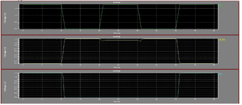
| A. Input & output waveform of conventional 6T SRAM cell |
| Power required by the conventional 6T SRAM cell during the above operation is 0.543μW in 0.18μm technology. |
 |
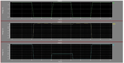
| B. Input & output waveform of proposed single bit-line 6T SRAM cell |
| Power required by the single bit-line 6T SRAM cell during the above operation is 0.432μW in 0.18μm technology. |
 |
CONCLUSION
|
| Technology development focuses on the limited use of the supply voltage in the electronic devices. Therefore, limiting the power consumption with new architectures are the design requirements in recent integrated circuits. In the case of SRAM, one seemingly counter intuitive approach is to utilize only a single bit-line without jeopardizing read stability, which leads to the development of a Single Ended 6T SRAM. Our paper mainly concentrates to reduce the power consumption in SRAM cell that can be used in the portable devices like PDA, cellular phones, portable multimedia devices etc. The proposed new SRAM cell gives a significant power reduction by reducing the switching voltage on bit lines. The power consumption is reduced in our project by reducing the switching voltage between the read and write operation. The dynamic power consumption of 40% to 60% of that of a conventional 6T SRAM cell is obtained. Power consumption is further reduced by employing the sweep transistor with the single bit-line 6T SRAM cell. |
| |
Figures at a glance
|
 |
 |
 |
 |
| Figure 1 |
Figure 2 |
Figure 3 |
Figure 4 |
 |
 |
 |
| Figure 5 |
Figure 6 |
Figure 7 |
|
References
|
- V.Subhamkari, G.S.Sivakumar,”Low Power Single Bit Line 6T SRAM Cell With read Stability”, International Journal Of Scientific &Engineering Research Volume4,Issue 7,July2013
- Gyanprakash, UmeshDutta,Mohd.Tauheed khan “Dynamic Power Reduction in SRAM”, International Journal Of Engineering Research And Applications,September 2012.
- Sunil kumar ojha&P.R.vaya “A Novel Architecture Of SRAM Cell For Low-Power Applications”.
- NeerajKr.Shukla,ManishaPattnaik,R.K.Singh,”Analysis Of The Data Stability And Leakage Power In The Various SRAM Cell Topologies”.
- Sheng lin, Yong Bin Kim, Fabrizio Combardi,”A 32nm SRAM Design For Low Power And High Stability”.
- Sapna Singh, Nehaarora, Nehagupta, Meenkshisuthar”simulation and analysis of 6T SRAM cell using power reduction techniques”, journal of engineering January 2012 .
- Behnmanamelifard,Farzanfallah,member,massoudpedram, fellow”leakage minimization of SRAM cells in a Dual-Vt and Dual-ToxTechnology”
- G.razavipour, a.afzali-kusha,m.pedram,”design and analysis of two Low powerbSAM cell structures”.
- S. Borkar, T. Karnik, S. Narendra, J.T schanz, A. Keshavarzi, and V.de, “Parameter Variations and Impact on Circuits & Microarchitecture," Proceedings of Design Automation Conerence., pp. 338-342, Jun.2003
- Jawar Singh, DhirajK.Pradhan et al,” A single ended 6T SRAM cell design for ultra low voltageapplications”,IEICE Electronic Express,2008,pp-750-755
- Yen Chen,Gary Chen et al., “A 0.6V dual rail compiler SRAM design on 45nm CMOS technology with Adaptive SRAM power for lower Vdd_minVLSIs,Solid-State Circuits, IEEE Journal,vol. 44 ,April.2009, Issue 4 , pp.1209-1214
- Koichi Takeda et al, “A Read Static Noise Margin Free SRAM cell for Low Vdd and High Speed Applications”,Solid-State Circuits, IEEEJournal vol. 41, Jan.2006, Issue 1 , pp.113-121
|