International Journal of Advanced Research in Electrical, Electronics and Instrumentation Engineering
ISSN ONLINE(2278-8875) PRINT (2320-3765)
ISSN ONLINE(2278-8875) PRINT (2320-3765)
Mallikarjun.P.Y 1, Dr.Y.S.Kumarswamy 2
|
| Related article at Pubmed, Scholar Google |
Visit for more related articles at International Journal of Advanced Research in Electrical, Electronics and Instrumentation Engineering
In order to reduce the length of global interconnection in 3D IC, Through Silicon via (TSV) provides an exact solution by providing high vertical interconnection density between device dies. TSV has some design issues such as IR drop, thermal dissipation, current delivery per package pin and several voltage domains among dies. To solve these issues, power network designs are used in 3D IC’s which plays an important role. We are going to propose a new integrated architecture of stacked-TSV and power distributed network [STDN]. This architecture provides three major roles such as power network to deliver larger current and reduce IR drop, Thermal network to reduce temperature and decoupling capacitor network to reduce power noise. Along with these roles, it also helps to overcome the limitation of the number of IO power pins. This STDN architecture is used for both single and multiple power domains to obtain good performance in 3D floor plan, IR drop, power noise, temperature, area and also the total length of signal connections for selected Microelectronics Centre of North Carolina[MCNC] benchmarks which can be simulated by using SPICE.
Keywords |
| 3D IC, TSV, STDN, IR drop, PGIO, PDN, SPD, MPD. |
INTRODUCTION |
| When compared to device and local interconnection, global interconnection in two dimensional (2D) system-on-chip (SOC) designs is not scaled as feature size of process technology which continuous to shrink. Therefore global interconnection has become an important design in these advanced technologies which yields high speed and power bottleneck with more functionality in one single chip [1]. Without further shrink of device sizes, three- dimensional (3D) integrated circuit (IC) chip has been founded as an effective way to obtain better performance in speed and power by scaled global interconnection. TSV provides high vertical interconnection density between device dies. But few of the design issues in TSV or even 3D IC from volumes of adoption such as IR drop, thermal dissipation, current delivery per package pin and various voltage domains among dies are obtained, which can be overcome by power network design. While performing network in 3DIC, traditional 2D design methodology is not suitable for 3DIC directly because of some new considerations such as: |
| ïÃâ÷ Power network partition: In multiple power domain (MPD) applications, 2D voltage island partition is not applicable to 3D dies/tiers because power mesh partition and TSV placement have to consider all dies at the same time in order to place level shifter. |
| ïÃâ÷ Thermal dissipation: Thermal TSV must be placed at location with maximum temperature gradient vertically among dies/tiers (3D approach) other than location with maximum temperature on the dies/tiers (2D approach), this is because location with maximum vertical temperature gradient is different from the location with maximum temperature in 3DIC.Therfore we can’t use 2D thermal approach [maximum temperature] to place thermal TSVs at hot spot directly. Power Distributed Network (PDN) a lonely is not effective way to reduce the temperature in 3D IC’s. Placement of PDN should take TSVs into considerations simultaneously for thermal dissipation path, since 2D flow is not able to consider power dissipation path among TSVs vertically. |
| ïÃâ÷ Limited number of power/ground IO pads: One of the important objectives in 3D IC’s is to reduce die area. Due to this reduction, only less number of power/ground IO pads (PGIO, IO pads in redistributed layer (RDL) or in package under bottom-most die connecting to power/ground voltage sources) and more current delivery per PGIO are required. It can be also defined as the placement of PGIOs in 2D approach without considering activities among all dies at the same time is not adequate. |
| This paper is mainly based on an integrated power network architecture Stacked TSV Distributed Network [STDN] proposed by Chen [2], and also proposes a power partition methodology in MPD of 3D IC to solve the above design issues. In this sense, our specific contributions in this work are summarized as follows. |
| ïÃâ÷ An extend 2D voltage island being suitable to 3D IC’s, voltage volume, is proposed. One of advantages in voltage volume of 3D IC is easier to place level shifters. |
| ïÃâ÷ Based on the STDN architecture, an algorithm to demonstrate the effectiveness of STDN for signal integrity and thermal dissipation in MPD is put forth. |
| The rest of the paper is organized as follows. Section 2 introduces motivation and previous works. Section 3 introduces the architecture of STDN. Section 4 shows 3D Floor Planning with New Proposed Architecture. Section 5 describes experimental setup. Conclusions are put forth in Section 6. |
II. MOTIVATION AND PREVIOUS WORK |
| Even though a lot of advantages in integrated circuit (IC) design by multiple power domains (MPD) [2] [3] or three dimensional (3D) IC [1] are proved, research work pays not much attention to MPD of 3D IC. To the best of our knowledge, there is no published research in MPD of 3D IC. On the contrary, there are several published researches on MPD of 2D IC design. The MPD technique for 2D IC can be applied in various stages of design flow - for example, floor- planning stage [6, 8], post-floor planning stage [2][4], placement stage [5], or post-placement stage [3] [6] [7]. J. Hu et al. [8] use a simulated annealing (SA) based algorithm to generate voltage islands on core-based 2D System-on- Chip (SoC) designs at the floor planning stage. After that, Hung et al. [9] combine genetic algorithm (GA) with SA, to take power reduction and thermal distribution into account at the same time. Mak and Chen [4] formulate the generation of voltage-island as an integer-linear-programming (ILP) problem whose objective is to reduce total power. Wu et al. [6] [7] propose an approximation algorithm to minimize the number of voltage islands. Ching et al. [3] then consider non-slicing voltage-island partitioning to facilitate the floor planning. Chang et al. use dynamic programming [10] and mixed integer linear programming (MILP) [2] to generate voltage islands in 2Dfloorplan with taking power network routing-resource, power reduction and speed degradation into consideration. Based on the above previous works, MPD is proved as a good method to reduce power with the same speed constraint in 2D IC’s. However, applying above MPD techniques of 2D IC to 3D IC’s |
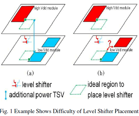 |
| makes the placement of level shifters Difficulty. For example, the level shifter cannot be placed at ideal region in Fig. 1 (a) because lacking of low supply voltage in upper tier and high supply voltage in lower tier. To solve this problem, an additional power TSV is required to distribute low supply voltage to upper tier, and it results in extra area and unpredictable changing to floor plan. In Fig. 1 (b), though the lower tier has two different supply voltages at the same time, we cannot precisely estimate the extra required power network routing resources of additional power mesh to transmit high supply voltage to ideal region. In this paper, we extend MPD to 3D IC design flow at floor planning stage. Unlike methodologies described above, we propose MILP-based algorithm in MPD of 3D IC. With considering impacts of TSV and characteristics of 3D IC, the proposed algorithm minimizes power and meets timing constraint at the same time. The vertical thermal dissipation is formulated in objective function to alleviate heat accumulation at tiers whose capability of thermal dissipation is poor. Based on the Ph.D. dissertation of Chen [10], even though a lot of researches on 3D IC, only two papers [7] [8] have discussed the design of power network in 3D IC. In [4], regular power distributed network (PDN) is constructed by top two layers of metal. As well, the fixed number of TSVs and fixed-pitch power mesh are used. In contrast, a co-synthesis of PDN and floor plan, which develops PDN and floor plan concurrently, in 3D IC’s, is proposed by [5]. In [5], both uniform and non-uniform PDN are constructed. In uniform PDN, there is only one PDN pitch for all tiers. In non-uniform PDN, each tier has its own optimal pitch without taking other tiers into account. The disadvantage of regular power distributed network [4] and uniform power distributed network [5] is that it cannot provide an optimal PDN pitch for a design which consists of active module with small area and inactive module with large area. For small and active module, a small PDN pitch is preferred; however, a large PDN pitch is preferred for large and inactive module. Non-uniform power distributed network proposed in [5] seems to be a better solution. Unfortunately, because pitch sizes among tiers are not considered, only limited number of TSVs can be placed to connect power networks among different tiers. For example, let the pitch of tier-1 be 157um and the pitch of tier-2 be 117um. Because TSV has to be placed at the common pitch location between tiers, the pitch for TSV between tier-1 and tier-2 will be 18369um. Inadequate interconnections (power TSVs) among power distributed network in different tiers will result in (1) more electron-migration issues, (2) more IR drop and (3) less efficiency in thermal dissipation. It is essential to bear in mind that thermal, signal integrity and reliability of 3D IC configurations are equally important. Algorithms looking into these issues have to consider the simultaneous interplay of all stacked tiers. In addition, because of low resistance, large capacitance, high current delivery and good thermal conductivity in the stacked-TSV, a well structure of PDN and stacked-TSV is a good candidate to solve the above design issues in 3D IC. Hence, to tackle the above issues, a novel integrated architecture of stacked-TSV and its corresponding power distributed network (STDN- Stacked TSV Distributed Network) [10] are applied. The STDN serves multiple roles to minimize IR drop, temperature and power noise. As well, it helps power delivery efficiency. Furthermore, a MILPbased construction of voltage volume is proposed to create MPD in 3D IC to reduce power and to meet timing constraint at the same time. |
III. NEW ARCHITECTURE OF STACKED-TSV AND DISTRIBUTED NETWORK |
| In this section, we introduce basic characteristics of the STDN (Stacked-TSV Distributed Network) [10] and compare it with other works [5] [10]. The description of STDN architecture is borrowed from PhD dissertation of Chen [10]. Structure of Stacked-TSV is as shown in Fig. 2 which illustrates the profile of stacked-TSV. The basic characteristics of the stacked-TSV are described as follows. |
| ïÃâ÷ TSV goes through silicon and stops on metal-1 (M1). M1 uses stacked via-array to connect top metal. |
| ïÃâ÷ Connection of tier-1 to package by RDL directly uses flip-chip method. Tier-1 to tier-2 is connected back-toback by bumping layer which also links TSV of tier-1 to TSV of tier-2. |
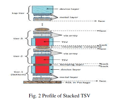 |
| ïÃâ÷ Tier-2 to tier-3 are connected face-to-back by inter metallic compound which links top metal of tier-2 to TSV of tier-3. The same interconnection is constructed between tier-3 to tier-4, tier-4 to tier-5, and so on except tier-(n-1) to top tier. 4. Tier-(n-1) to top tier is connected face-to-face by inter metallic compound which links top metal of tier-(n-1) to top metal of top tier. This structure allows that the top tier does not need TSV process. 5. All of power/ground (PG) sources are connected through RDL to PG nodes of tier-1, while the PG nodes in upper tiers are connected to PG sources by TSVs of tier-1. 6. Stacked-TSV has two sizes- 6um and 8um in diameter. 7. Taking 3 tiers as an example. To serve as power TSVs and thermal TSVs, the stacked- TSVs could be connected in two ways: (1) tier-1 to tier-2; (2) tier-1 to tier-2 to tier-3. To serve as DECAP (decoupling capacitor) TSVs, the stacked-TSVs could be connected in three ways: (1) tier- 1 to tier-2; (2) tier-1 to tier-2 to tier-3; (3) tier-2 to tier-3. |
| Next, the basic characteristics of the STDN are described as follows: |
| ïÃâ÷ Power network are constructed by top two layers of metals. |
| ïÃâ÷ The space between power and ground is half of tier-1's pitch for all tiers. |
| ïÃâ÷ The pitch ratio of tier-1: tier-2: tier-3: tier-4 is 1:2:4:4. This is a key property of the power network. With this property, stacked-TSVs connecting power networks in different tiers can be inserted easily. The actual pitch size is determined by module activities, IR drop, thermal dissipation and floor plan during floor planning. |
| ïÃâ÷ Stacked-TSVs are placed on cross section optionally. |
| ïÃâ÷ STDN uses two metal widths in power network- 8um and 10um. Technically speaking, there is 1um enclosure space of PG mesh to stacked-TSV. |
| ïÃâ÷ For the purposes of manufacturing yield, the sizes of all stacked-TSVs in one design are the same. |
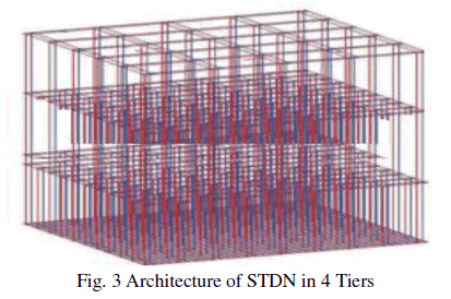
| An example of STDN in 4 tiers is illustrated in Fig. 3. The planar lines in red are power mesh and the planar lines in blue are ground mesh. The vertical bars in red are TSVs connected to power mesh while the vertical bars in blue are TSVs connected to ground mesh. |
 |
A. COMPARISON WITH OTHER POWER DISTRIBUTED NET-WORKS |
| First of all, stacked-TSV structure is compared with other TSV structures. In [11], the bottom-most tier connects TSVs to solder bump directly and top-most tiers uses top metal to connect top metal of lower tier. The disadvantage of this method is that the area of bottom-most tier is larger than other tiers because the pitch of solder bump is larger than TSV. In this approach, stacked-TSV uses RDL (flip-chip) to connect bottom-most tier. It results in smaller area in bottom-most tier because the pitch of RDL is smaller than the pitch of solder bump. The top-most tier connection approach in [4] is the same as one in [11]. However, the thermal dissipation is more effective in [4] than that in [11] because TSV uses copper and RDL uses aluminium. In [4], the bottom-most tier connection is the same as [11]. However, it needs TSVs in top-most tier while [10]'s and [11]'s do not. Secondly, we compare PDN structure in the STDN to other power distributed networks. In [5], both uniform and non-uniform PDN are constructed. In uniform PDN, there is only one PDN pitch for all tiers. The disadvantage of this method is that it cannot provide an optimal PDN pitch for a design which consists of active module with small area and inactive module with large area. For small and active module, a small PDN pitch is preferred; however, a large PDN pitch is preferred for large and inactive module. As to the STDN, the pitch of lower tier is smaller than the pitch of upper tier. The most active module will be placed at bottom-most tier which is near thermal sink and power sources. On the other hand, in non-uniform PDN, each tier has its own optimal pitch without taking other tiers into account. The disadvantage of this method is that the number of TSVs is unpredictable because TSV has to be placed at the common pitch location between tiers. For example, if the pitch of tier-1 is 157um and the pitch of tier-2 is 117um, the pitch for TSV between tier-1 and tier-2 will be 18369um. If length of chip is smaller than 18369um then there is no TSV between tiers. As regards STDN, it applies regular proportional pitches (i.e., 1:2:4:4) among tiers. The lower tier has more number of power strips in STDN to place active blocks because both power sources and heat spreaders are placed under bottom-most tier. In [4], the structure of PDN and the number of TSVs are predefined. Not only the metal width of PDN is predefined but also the metal pitch of PDN. The disadvantage of this method is that uneven module activities are not taken into account. In STDN, both the metal width and the size of stacked-TSVs are predefined; however, the PDN pitch in STDN is optimized based on module activity, IR drop and thermal dissipation requirements during floor planning. |
| In summary, the major advantages of the STDN architecture [10] are: |
| ïÃâ÷ Based on regular PDN mesh and the ratios of pitches which are given constants among tiers, the number of TSVs in stacked-TSV architecture and the length of PDN are well controlled by PG mesh pitch. Moreover, all of stacked-TSVs are the same size and aligned. It is friendly to process manufacturing for variation control. |
| ïÃâ÷ All of current deliveries are uniformly shared by STDN. It helps alleviating the limitation of the number of PGIOs and reducing electron migration impact. |
| ïÃâ÷ A key observation in [6] shows both the number of PGIOs and the number of TSVs in each layer being increased (decreased) at the same time according to PDN mesh pitch maximizes the performance in power noise reduction. The STDN architecture meets this requirement. |
| ïÃâ÷ Because of well controlled pitch in STDN, thermal wire is able to conduct thermal lateral to the nearest stacked-TSVs for thermal dissipation effectively. |
| ïÃâ÷ Because STDN plays dual roles in power network and thermal network, refinement of STDN reduces IR drop and temperature at the same time. |
IV. 3D FLOOR PLANNING WITH NEW PROPOSED ARCHITECTURE |
| To demonstrate the effectiveness of multiple power domain (MPD) technique in 3D IC, we develop an algorithm, which co-synthesizes floor plan, the STDN (Stacked-TSV Distributed Network) [10] and voltage volume. As to the proposed algorithm, our objective is to minimize IR drop, to minimize temperature, to reduce power consumption and to meet performance constraint simultaneously. The output includes floor planning result (including module placement and construction of STDN) and the actual size of power distributed network (PDN) pitch under given pitch ratios among tiers. |
A. PROBLEM FORMULATION |
| In order to describe problem formulation clearly, multiple power domain (MPD) problem is separated from single power domain (SPD) problem even though those two problems are solved by the same algorithm in a fusion way. |
| • Problem of single power domain is defined as follows: |
| Given a set of current consumption for each module, a net-list of module connectivity in block-level, geometry information of each module (length, width of module, locations of pins, etc.) and the number of tiers for 3D floor plan. Our objective is to floor plan those modules and construct power distributed network by STDN so that IR drop, temperature, area, wire length and the number of signal TSVs are minimized. |
| • Problem of multiple power domains is defined as follows: |
| Given a set of current consumption for each module, a net-list of module connectivity in block-level, geometry information of each module, the number of tiers for 3D floor plan, timing constraints and the number of voltages used. Our objective is to floor plan those modules, construct power distributed network by STDN and assign voltages to modules so that IR drop, temperature, area, wire length, the number of signal TSVs, the number of level shifters, total power consumption are minimized and timing constraints are met. |
B. Voltage Volume |
| The concept of voltage volume in 3D IC is similar to voltage Island in 2D IC. As is implied by its name, the modules applied the same voltage are placed at the same planar (2D) location among all tiers such that STDN [10] are partitioned to cut power mesh and the corresponding Stacked-TSVs are able to connect to the same voltage. Fig. 4 demonstrates an example of 3D floor plan with voltage volume in multiple power domain of STDN. The modules in the same color are assigned to the same voltage. |
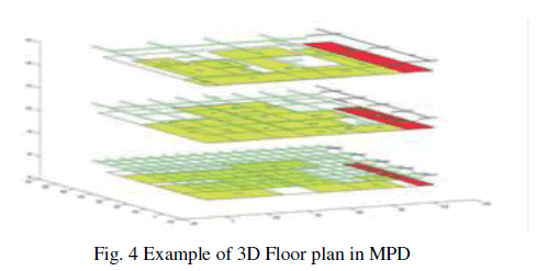 |
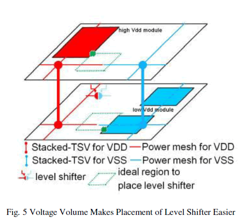
| The lines of the same colour are PDN in the same voltage. In the STDN architecture, ground pins of module are connected to the common ground STDN. So, we only need to partition STDN into different supply voltages. For example, in Fig. 4, two kinds of power voltages and one ground voltage are supplied for tiers. It results in two voltage volumes. In order to avoid large leakage in standard cell, a level shifter is required when signal propagates from low voltage to high voltage. One of key advantages of voltage volume is that level shifters are easily to be placed at any tier. Because each tier is partitioned into voltage volume according to the number of voltages used, each tier has all its required voltage levels. The two power supply voltages of level shifter are able to be connected at the same tier where level shifter is placed. Without the concept of voltage volume, it is very difficult to place level shifters as shown in Fig. 1. An example shown in Fig. 5. Illustrates how voltage volume benefits the placement of level shifters. With the concept of voltage volume, all required voltages are promised to exist near the ideal region of level shifter. In this way, the extra routing resource of power network required for transmitting supply voltage to ideal region is under control. |
 |
C. IR DROP MODELLING |
| STDN [10] builds electrical resistors and capacitors based on distributed network geometry while considering power pins of each module as current sources. Based on master's thesis of Wang [5], we analyse circuit in two approaches such as DC IR drop analysis and Transient IR drop analysis. For DC IR drop analysis, resistance of stacked- TSV, resistance of PDN in STDN and constant currents are applied. For power noise analysis (transient IR drop), STDN takes resistance, capacitance and transient current stimuli into consideration. In addition to resistors, capacitors and current sources, ideal voltage sources are applied from IO pads through bottom-most tier as power sources. In IR drop modelling, both RDL and package are not taken into account for all simulations (including ours and [5] emulations). In other words, ideal voltage sources are directly connected to passivation opening in flip-chip of bottom-most tier. As to power noise analysis (transient IR drop), the waveform of transient current stimulus is approximated by a triangular waveform to emulate current transitions during voltage transitions of signals. The total charge of transient current waveform is equal to total charge of DC (constant) current waveform. This relationship is formulated as given in Equation. (1). |
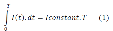 |
| Where, I (t) is transient current stimuli, I constant is constant current and T is simulation time. After 3D floor plan and STDN construction is done, a SPICE simulation run deck and SPICE net-list are generated. Then HSPICE simulator [7] is invoked to simulate run deck and to output IR drop measurement data. |
D. THERMAL MODELLING |
STDN [11] builds an equivalent thermal circuit through thermal-electrical analogy. By steady-state equations of thermal network, thermal resistors are connected between spatially adjacent nodes. Moreover, thermal current sources are mapped to power sources. Assumed that the power consumption of each module is distributed evenly, power consumption of each thermal grid is calculated by counting the overlapping area among grid and modules. For example, total power consumptions of module mi and mj are pi, pj respectively. If each of them with half area inside the thermal grid TGk then power consumption in grid TGk, is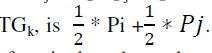 . The voltages at the nodes in this equivalent thermal circuit are computed by solving equations of equivalent thermal network. These voltages yield the temperatures at those nodes. The ground node of the circuit corresponds to a constant temperature node; this is typically the ambient temperature. In this thermal modelling of STDN, grid-based method is applied for thermal simulations and analysis. 20 × 20 grids are used in thermal network laterally. Based on the above approach, all thermal resistors, voltage sources for ambient temperature, current sources for power consumptions are generated into SPICE run deck and net-list. As does IR drop simulation, HSPICE simulator is applied to simulate and to output temperature measurement data. . The voltages at the nodes in this equivalent thermal circuit are computed by solving equations of equivalent thermal network. These voltages yield the temperatures at those nodes. The ground node of the circuit corresponds to a constant temperature node; this is typically the ambient temperature. In this thermal modelling of STDN, grid-based method is applied for thermal simulations and analysis. 20 × 20 grids are used in thermal network laterally. Based on the above approach, all thermal resistors, voltage sources for ambient temperature, current sources for power consumptions are generated into SPICE run deck and net-list. As does IR drop simulation, HSPICE simulator is applied to simulate and to output temperature measurement data. |
E. SIMULATED ANNEALING BASED FLOOR PLANNING ALGORITHM |
| In order to trade off many design factors in 3D floor plan at the same time, nondeterministic algorithm, simulated annealing (SA), is used in our algorithm as shown in Fig. 6. |
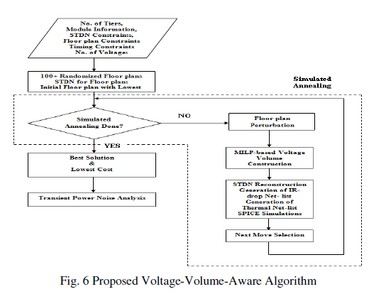 |
| In addition, 3D B-tree structure is applied in our algorithm as a floor plan representation [5]. First, the number of tiers in 3D floor plan, module information (power consumption, net list, width, length, pins, etc.), the size of stacked-TSV, and the width of PDN in STDN, range of PDN pitch, IR drop and EM limitations are fed into flow. Furthermore, if 3Dfloor plan is constructed in multiple power domains (MPD) the timing constraints and the number of voltages applied in MPD are also fed into flow. Second, hundreds of 3D floor plan of the selected benchmark is randomly generated and the corresponding STDN structures are constructed accordingly. Based on our cost function, the best floor plan with the corresponding lowest cost is found among those hundreds of random floor plans as an initial solution. In single power domain (SPD), the cost factors in cost function include maximum IR drop, maximum temperature, and maximum temperature gradient, maximum area variation, footprint area, the number of stacked-TSVS in STDN, the number of TSVs for signals, total wire length of signals, total wire length of STDN and white space. White space is defined as area not used by module in core area (it might be used by power strips in STDN and stacked- TSVs outside of modules). In multiple power domain (MPD), besides the cost factors defined in single power domain, the cost factors in cost function include the number of level shifters, area of level shifters and product of power and delay. Third, simulated annealing (SA), a non-deterministic algorithm, is applied as a main body of our algorithm to find lowest cost solution. Fourth, the perturbation of the current floor plan and STDN is created. The perturbation consists of inter-tier movement, inter tier swapping, intra-tier movement, intra-tier swapping, intra-tier rotation and pitch refinement. Fifth, if 3D floor plan is MPD, voltage volume (i.e., voltage domain partition) is constructed. Then Integer Linear Programming (ILP) is applied for voltage assignment [8]. Sixth, the SPICE run decks and net-lists (both DC and transient) are constructed according to 3D floor plan and STDN structure for IR-drop and thermal simulations. Seventh, SA selection method is used with HSPICE simulation results. Finally, when the simulated annealing process terminates, transient power noise (transient IR drop analysis taking both resistance and capacitance into account) is analysed for the generated floor plan and STDN. If transient power noise of node is larger than a predefined threshold (10% VDD in our algorithm), the stacked- TSVs, serving as decoupling capacitors, are added in STDN around nodes which violates power noise threshold. |
V EXPERIMENT SETUP |
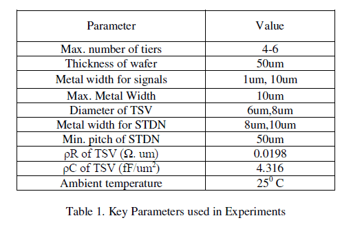
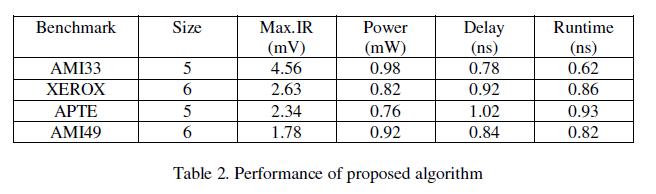
| Four benchmark examples (AMI33, XEROX, APTE and AMI49) selected from MCNC benchmarks are used in our new architecture for 3D floor plan experiments. The number of tiers varies from 1 to 4 for each benchmark. The CMOS BULK process with copper TSV and metal layers in 90nm technology is applied in experiments. As to 3D floor plan in single power domain, 1V typical voltage is applied. As regards 3D floor plan in multiple power domains, three voltages (0.8V, 1.0V, 1.2V) are applied. When the number of tier is one, the flip chip with 2 times STDN pitch is applied to connect power pads. In other words, flip chip pitch is 100um while STDN pitch is 50um. If maximum IR drop and ground bouncing is larger than 15% of VDD, then the metal width of power pin of the module to STDN is redefined to 10um (the width is 1um by default for power pins of the modules). The key parameters used in experiments are summarized as shown in Table 1, where ρR is resistivity and ρC is capacitance per unit area. Table 2 shows the performance of proposed algorithm using various benchmarks. |
 |
 |
VI. CONCLUSION |
| A new integrated architecture, STDN (Stacked TSV Distributed Network), is developed to create 3D floor plan and its distributed network for power delivery and thermal dissipation at the same time. It presents its effectiveness in solving IR drop, temperature, power noise and floor plan quality. Furthermore, voltage volume is proved as an effective approach in multiple power domains partitioning for 3D floor plan. |
References |
|