International Journal of Innovative Research in Computer and Communication Engineering
ISSN ONLINE(2320-9801) PRINT (2320-9798)
ISSN ONLINE(2320-9801) PRINT (2320-9798)
Sandeep Khichar 1, Laxmikant Paptan 2, Sukoon Mishra3, Akriti Singhal4
|
| Related article at Pubmed, Scholar Google |
Visit for more related articles at International Journal of Innovative Research in Computer and Communication Engineering
Strained silicon devices are one of the most important Technology Enhancers for further Si CMOS developments. The mobility enhancement which is obtained by applying appropriate strain provides higher charge carrier velocity in MOS channels, resulting in a higher current output under a fixed supply voltage (V) and gate oxide thickness (tox).The mechanism of mobility enhancement, methods of strain generation, challenges and drawbacks, improvements and key issues of strained silicon devices and their application for advanced VLSI devices is reviewed in this paper.
Keywords |
| strained silicon, mobility enhancement, process-induced strain, global strain, SSOI |
INTRODUCTION |
| The ordinary device scaling was the most important principle of performance enhancement in Si CMOS for more than 30 years. However, starting with 90 nm technologies the performance enhancements of CMOS started to diminish through standard device scaling such as shrinking the gate length and thinning the gate oxide due to several physical limitations in miniaturization of MOSFETs. For example, thinning the gate oxide requires a reduction of the supply voltage and an increase of the gate tunnelling current occurs. Furthermore, raising the dopant concentration in the substrate is substantial to suppress short channel effects that decrease the carrier mobility and drive current, respectively. |
| Thus, new channel structures and materials, which mitigate the stringent constraints regarding the device design, have recently stirred a strong interest. These so-called Technology Boosters [1] include strained silicon channels, ultrathin SOI, metal gate electrodes, multigate structures, ballistic transport channels, as well as others. Among them, strained silicon channels have been recognized as a technology applicable to near term technology nodes [2 - 4]. The mobility enhancement obtained by applying appropriate strain provides higher carrier velocity in MOS channels and drive current, respectively, at the same supply voltage and gate oxide thickness. It implies that thicker gate oxides and/or lower supply voltage needs to be used for a fixed drive current, leading to the mitigation of the trade-off relationship among drive current, power consumption and short-channel effects. |
| This paper presents the principle, the fabrication, and device applications of strained silicon with an emphasis on the physical mechanism of the carrier mobility enhancement due to strain. |
II. BASIC THEORY |
Physical Mechanism of Mobility Enhancement in Strained Silicon |
| The inversion layer mobility in Si MOSFETs is a physical parameter to describe the drain current and to study the electric properties of a 2-dimensional carrier system. It has already been reported that the electron and hole mobilities in the inversion layer on a (100) surface follow universal curves at room temperature independent on the substrate dopant concentration or the substrate bias when plotted as a function of effective normal field Eeff [5,6] In weak inversion Coulomb scattering dominates. Increasing Eeff causes acoustic phonon scattering to dominate the mobility, which decreases withïÃâ¬Ã Ã¯ÃâõphononïÃâ¬Ã ∝ Eeff-0.3. For the highest Eeff, both surface- roughness scattering and phonon scattering are active, andïÃâ¬Ã Ã¯Ãâõeff decreases more tremendously (ïÃâõSRïÃâ¬Ã ∝ïÃâ¬Ã Eeff-2 for electrons andïÃâ¬Ã Ã¯ÃâõSRïÃâ¬Ã ∝ Eeff-1 for holes). MOSFETs operating with high mobilities in the low Eeff range to use the full performance advantage and get the highest drive current. Therefore a high channel doping is needed to control the threshold voltage VT in planargeometry, short-channel devices. The high Eeff and lowïÃâ¬Ã Ã¯Ãâõeff of inversion carriers in MOSFETs is an unfavourable effect of channel length scaling. Therefore, the advantage of strained silicon relies in its ability to fundamentally alter the band structure in ways that increase the effective mobilityïÃâ¬Ã Ã¯Ãâõeff. |
| The effect of strain on the band structure of silicon and on the carrier mobility was extensively studied for more than two decades [7]. Mobility improvement in strained silicon takes place mainly due to |
| a) The reduction of the carrier conductivity effective mass, and |
| b) The reduction in the intervalley phonon scattering rates. |
| The conduction band of unstrained bulk silicon has 6 equivalent valleys along the <100> direction of the Brilloun zone, and the constant energy surface is ellipsoidal with the transverse effective mass, mt = 0.19m0, and the longitudinal effective mass, ml = 0.916m0 [8]. In the inversion layer on a (100) surface, these 6 valleys are split into the 2-fold degenerate valleys with ml perpendicular to the Si/SiO2 interface and the 4-fold degenerate in-plane valleys with mt. If strain is applied, the energy of the conduction band minima of the 4-fold valleys on the in-plane <100> axes rises with respect to the energy of the 2-fold valleys on the <100> axes perpendicular to the plane. As a consequence, the electrons prefer to populate the lower valleys, which are energetically favoured. This result in an increased electron mobility via a reduced in-plane and increased out-of-plane electron conductivity mass. For a given strain, quantifying the effective mass reduction and comparing it to the enhanced mobility reveals that mass reduction alone explains only part of the mobility enhancement [8]. Hence, electron scattering must also be reduced due to the conduction valleys splitting into two sets of energy levels, which lowers the rate of intervalley phonon scattering. Many types of strain increase the electron mobility such as in-plane biaxial and uniaxial tensile and out-of-plane uniaxial compressive strain. |
| For holes, the valence band structure of silicon is more complex than the conduction band. It is the complex band structure as well as valence band warping under strain [7] that result in a much larger hole than electron mobility enhancement. The band warping is also responsible for the fact that different types of strain (biaxial tensile and uniaxial compressive) behave differently. For unstrained silicon at room temperature, holes occupy the top two bands; the heavy and light hole bands [9]. Applying strain, the hole effective mass becomes highly anisotropic due to band warping, and the energy levels become mixtures of the pure heavy, light, and split-off bands. Thus, the light and heavy hole bands lose their meaning, and holes increasingly occupy the top band at higher strain due to the energy splitting. Important to achieving high hole mobility is a low in-plane conductivity mass for the top band. In addition to a low inplane mass, a high density of states in the top band and a sufficient band splitting to populate the top band are also required. Uniaxial compressive strain on both (100) and (110) surfaces, for instance, create a high density of states in the plane of the MOSFET. |
Methods of strain generation |
| There are generally two different methods to introduce strain in the channel region: biaxial strain and uniaxial strain. Biaxial strain is also referred to as global strain and is introduced by epitaxial growth of Si and SiGe layers (substrate engineering). The strain is induced by the lattice mismatch between Si and SiGe. The advantages of SOI and biaxially strained silicon layers can be combined in a single substrate of strained silicon on insulator (SSOI). Uniaxial strain is generated by local structural elements near the channel region. Since these process modules that cause uniaxial strain are part of high performance CMOS processes, uniaxial strain is also referred to as process-induced strain (PIS). Owing to the relative ease of integrating process-induced strain modules in conventional CMOS processes, strain enhanced scaling has relied on the development of new advanced methods of PIS. The application of local strain elements, however, is limited by further scaling making some of them ineffective or unfeasible. |
Local Strain (Process-Induced Strain). |
| Electron and hole mobilities respond to mechanical stresses in different ways. For MOSFETs with the [110] channel orientation on (001)-oriented silicon substrates, tensile strain along the [110] direction improves electron mobility but degrades hole mobility. Therefore, to improve both the electron mobility in n-channel MOSFETs (NMOS) and the hole mobility in p-channel MOSFETs (PMOS), different approaches for strain inducement in the p- and n-channel transistor is needed. |
| Advanced CMOS processes include different process-induced stressors. These are mainly stressed contact layers, embedded stressors, and stress memorization techniques (Fig. 1). Contact layers are typically stressed nitride layers deposited after salicidation on the top of devices. Tensile contact layers are deposited on NMOS and compressive contact layers are deposited for PMOS. |
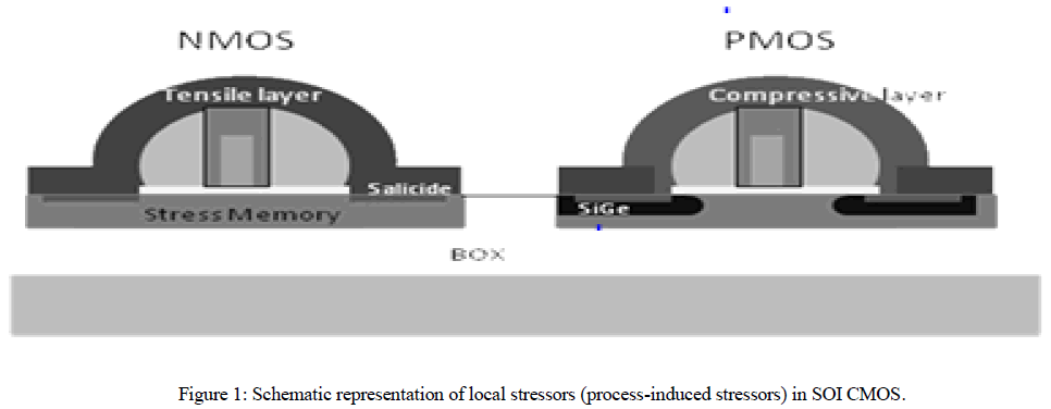 |
| Tensile strain in NMOS is obtained by tensile contact layers and various stress memorization techniques. Compressive strain in PMOS is induced by compressive contact layers and embedded SiGe. |
| The strain in the channel region depends on the intrinsic stress of the layer, thickness of the layer, and device dimensions. Using tensile and compressive contact layers (dual stress liner, DSL) a significant hole mobility enhancement of 60% was achieved [10]. Furthermore, important parameters of SOI CMOS devices, such as effective drive current enhancement, were proved in different 45 nm technologies. |
| Stress memorization techniques (SMT) typically involve a pre-amorphization, a nitride capping layer and an additional annealing process. SMT increases the NMOS drive current and degrade the PMOS device performance. |
| Embedded SiGe layers (eSiGe) are used in PMOS transistors. Due to the larger lattice constant of SiGe compared to silicon, a compressive strain is induced in the channel of the PFET. This technique can be optimized and improved by combining SiGe and SiC layers for CMOS devices [11, 12] . |
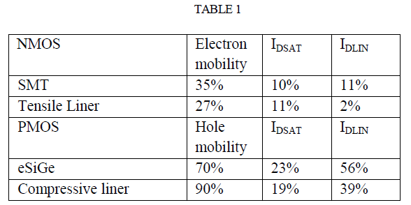
| The integration of the different stressors into advanced CMOS technologies results in increasing device performance required by the ITRI road map [1]. Typical effects of local stressors on the carrier mobility and the drive current (saturation drive current IDSAT and linear drive current IDLIN) are summarized in Table 1 for SOI CMOS devices [13]. |
 |
Global Strain. |
| Global strain on wafer level is induced by the epitaxial growth of Si1-x Gex and Si layers. Because the lattice constant of Si1-x Gex (0 ïÃâã x ïÃâã 1) alloys varies between 0.5431 nm for silicon (x = 0) and 0.5657 nm for germanium (x = 1) tensile strain is induced in a silicon layer epitaxially grown on top of the SiGe. The strain is generally biaxial. Furthermore, uniaxial strained layers can also be obtained by mechanical straining. |
Biaxially strained layers. |
| Various heterostructure substrates have been applied to realize biaxial strain and high-mobility channel materials [16]. Epitaxially grown Si1-x Gex layers on Si bulk wafers are generally applied acting as substrate for a strained silicon layer grown on top (bulk materials). In order to reduce the defect density in the strained silicon a relaxed Si1-x Gex buffer is required grown on a graded Si1-x Gex layer. Because the Ge concentration x increases continuously by about 10 % per μm, the thickness of the graded buffer is several micrometers. An alternative is the relaxation of a thin pseudomorphic SiGe layer (< 500nm) induced by hydrogen or helium implantation and subsequent annealing [17]. A thinner SiGe buffer makes the process cost effective. Variations of the basic structure have also been published including dual channel structures incorporating an additional strained Si1-y Gey layer with y > x and heterostructures on bulk using a second strained silicon layer [15]. Layer stacks of the different types have been applied as virtual substrates for the preparation of SSOI and SGOI wafers. |
| The realization of SSOI wafers from bulk materials is a complex process combining wafer bonding, layer transfer, and etch-back methods. The SSOI technologies provide a pathway to implementing mobility enhancement in partially or fully depleted devices, in ultrathin-body MOSFETs, or nonplanar (double-gate) MOSFETs. Furthermore, long channel devices (Lg ïÃâó 1μm) show clearly improvements of the device characteristics. For instance, drive current (IDSAT) improvements of 80% at the same source-to-drain leakage (IOFF) has been measured. Improvements in the same order of magnitude were not obtained for short channel devices. Here, an IDAST improvement of only 10 - 20% was obtained up to now [17]. The main reason was the interaction with process-induced stressors reducing the effect of the biaxial strain [18]. This means that applications of SSOI wafers require modifications of existing CMOS processes. The combination of biaxially strained SSOI and optimized uniaxial stressors (dual-stress nitride capping layer and embedded SiGe) was already demonstrated resulting in IDSAT improvements of 27% and 36% for n- channel MOSFETs and p-channel MOSFETs, respectively, in sub- 40 nm devices [19]. In addition, the gate leakage current was also reduced by 30%. All investigations suggest that the combination of biaxially strained SSOI and uniaxial strain by process-induced stressors is the optimum way for future requirements [15, 18, 19]. |
Uniaxial strained layers: |
| Two wafers were bent over a cylinder thereby creating a curved or bowed wafer with a strained state induced. The bending direction was parallel to [110]. The curved wafers are brought into contact via direct wafer bonding and covalent bonds across the bonded interface form upon annealing in the bent state. By combining the process with hydrogen-induced layer splitting thin strained layers were transferred. The process can generally be used to realize strained layers of either tensile or compressive strain. The strain introduced by this technique is significantly lower as for biaxially strained layers. Depending on the radius of curvature strain values between about 0.08% and 0.04% were obtained for a radius of curvature ranging from 0.5 m up to 1 m. |
Mobility Enhancement for Future Devices |
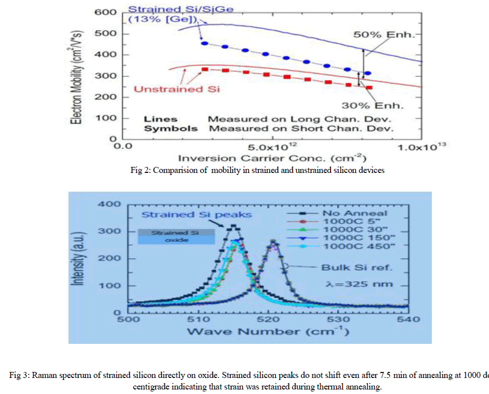
| Numerous experiments over the last years proved the applicability of biaxially strained silicon in state-of-the-art device processes. Mobility enhancement of 50 % for electrons (with 15 % Ge) and 15 - 20 % for holes (with 20-25% Ge) has been demonstrated. An alternative process to attain SiGe layers with higher Ge content, i.e. higher strain in the upper strained silicon layer, is the Ge condensation method. The process consists of epitaxial growth of a strained SiGe layer with a low Ge fraction on a SOI substrate and successive high-temperature oxidation. SiGe layers having Ge fractions of more than 0.5 and large strain values over 1 % were realized. A hole mobility enhancement by a factor of 10 was measured. Recently, however, variations of the threshold voltage are obtained on SGOI-MOSFETs fabricated by the Ge condensation process. |
| The strained silicon on insulator (SSOI) without a buried SiGe layer appears to be more favourable. This is also true with respect to the process integration. Associated with the presence of the SiGe layer below the channel, such as Ge segregation at the Si/SiO2 interface, enhanced As or P diffusion, limited thermal budget, and rapid dopant diffusion along misfit dislocations, would be largely eliminated [9]. Most of the measurements reported up to now, however, show enhanced mobility data and drive current improvements only on long-channel devices which cannot reproduced in the same order for short-channel devices having gate lengths of 60 nm and below . As described above, the main reason was the interaction with process-induced stressors reducing the effect of the biaxial strain [18]. Process integration of SSOI materials in CMOS technologies is therefore an important issue. |
| The advantage of SSOI is the scalability to thinner device and insulator (BOX) layers, respectively. This allows the combination of strain with benefits of ultrathin-body (UTB) MOSFETs. |
Challenges of Strained Si on SiGe |
| 1. Increased Junction Capacitance and Leakage (due to Higher Dielectric Constant and Lower Band Gap). |
| 2. Reduced thermal conductivity (15x) of SiGe (Self heating) |
| 3. Short Channel Effects |
| 4. Dislocations (>105/cm2) |
| 5. Integration of NMOS and PMOS |
| 6. Enhanced As,P diffusion (Smaller Leff for a given Lpoly) |
| 7. Parasitic hole channel at strained SiGe/Si Interface |
Ways to reduce Dislocation Density |
| 1. Optimize grade (~10%Ge/um) temperature |
| 2. Restricted geometry |
| 3. CMP (Reduced Pile-Up: Less dislocation relieve the same stress). |
| Decreasing the layer thickness conserves the strain even for small structure sizes. This means that at thicknesses of the strained silicon layer below 10 nm (required for UTB SSOI MOSFETs) and gate length in the sub- nanometre range the whole tensile strain is preserved. Under specific conditions simultaneously devices with different stress behaviour (tensile or compressive) within one device may exist by applying biaxially strained SSOI wafers. The results of the simulation were experimentally verified by Raman measurements [20]. In addition, Raman and TEM analyses also proved the transformation of the biaxial into uniaxial strain by increasing the ratio of the width to the length of structures. This implies also the use of the advantages of uniaxial strain for device performance enhancement [20]. |
 |
Thermal Stability to Subsequent Processing |
| - Ge Diffusion: 2(Dt)1/2~6 nm for 1h at 900 C. Activation Energy 3.3 eV. |
| - Strain Relaxation: Undetectable after 850 C 1h anneal. RTA at higher temperatures possible Key Issues |
| - Growth rate is key for production-worthiness. |
| - Defect Density is critical. The graded layer approach leaves the defects in the bottom layer. A defect-free strained layer is thus achieved. |
Advantages |
| Bulk electron and hole mobility is enhanced in Strained Si: |
| For p-MOSFET, hole mobility increases for Ge content up to 30-40%, while for n-MOSFET, the electron mobility saturates at about 20% of Ge. |
Reported improvements |
| • Electron mobilities > 70 % on bulk Si NMOS is reported by IBM. |
| • Electron mobilities of > 50 % and hole mobilities 15-20 % on SOI is reported by IBM. |
| • Electron mobilities of 1.7x on SOI are reported by Hoyt (IEEE El. Dev.Letr'01). |
| • Electron mobilities > 75 % on bulk Si is reported by Hoyt, Gibbons & Rim (IEEE Trans,’00). |
Key Issues |
| 1. Gate oxidation |
| 2. Device Isolation |
| 3. Self Heating |
| 4. Growth rate cost |
| 5. Defect density at surface |
| 6. Process integration difficulties |
III. CONCLUSION |
| Strained silicon devices are one of the most important Technology enhancers for further Si CMOS developments. The mobility enhancement obtained by applying appropriate strain provides higher charge carrier velocity in MOS channels, resulting in higher output current under a fixed supply voltage and gate oxide thickness. Process-induced stress including tensile or compressive stress and various stress memorization techniques are already integrated in today´s high performance technologies. The application of local strain elements, however, is limited by further scaling. On the other hand, one of the most important advantages of globally strained SSOI is the scalability to thinner device and insulator layers. This allows the combination of strain with benefits of ultrathin- body (UTB) MOSFETs. The reduction of the thickness of the silicon layer contributes to the strain. Furthermore, varying the relation between channel length and layer thickness can introduce both types of strain and the modification from of the biaxial into uniaxial strain. Also there are some challenges and drawbacks which must be overcome to fully utilize the improvements of strained silicon technology. |
References |
|