International Journal of Advanced Research in Electrical, Electronics and Instrumentation Engineering
ISSN ONLINE(2278-8875) PRINT (2320-3765)
ISSN ONLINE(2278-8875) PRINT (2320-3765)
Saradindu Panda1, B.Maji2, Dr.A.K.Mukhopadhyay3
|
| Related article at Pubmed, Scholar Google |
Visit for more related articles at International Journal of Advanced Research in Electrical, Electronics and Instrumentation Engineering
This paper describes the design issues of DRAM, simulation of 3T DRAM cell, and measurement of its power and delay, for various channel length. Varying the parameters such as channel length, we observe different results being reflected in its power and delay which is described in this paper. Waveforms are plotted as per our observations.
Keywords |
| 3T DRAM, Power, Delay, Channel Length. |
INTRODUCTION |
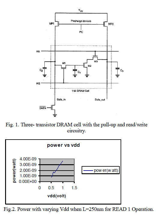
| THE ever increasing demand for reliable electronic equipment of smaller size and low power requirement in communication, computers and aerospace industries has led to the growth of circuit microminiaturization. Semiconductor memory is an electronic device to store the data, often used as the memory of computer, implemented on a semiconductor based integrated circuit. A three transistor DRAM cell consist of column pull up (pre-charge) transistors and the column read/write circuitry. Here the binary information is stored in the form of charge in the parasitic node capacitance C1.The storage transistor M2 is turned on or off depending on the charge stored in C1, and the pass transistors M1 and M3 act as access switches for data read and write operations. The cell has two separate bit lines data read and data write, and two separate word line to control the access transistors. A simplified 3T DRAM Cell is shown in Fig 1. |
II. OPERATING PRINCIPLES OF 3T DRAM CELL |
| The operation of the 3T dram cell and its peripheral circuitry is based on a two phase non-overlapping clock scheme. Every data read and data write operation is preceded by a pre charge cycle, which is initiated with the pre charge signal PC going high. During the pre charge cycle the column pull transistors are activated and the corresponding column capacitances are charged up to logic –high level. |
| All data read and write operations are performed during the active phase i.e. when PC is low. |
| For the write one operation the inverse data input is at the logic-low level, because the data to be written onto the DRAM cell is logic “1”.Consequently, the “data write” transistor MD is turned off, and the voltage level on column Din remain s high. Now, the “write select” signal Ws is pulled high during the active phase. As a result, the write access transistor M1 turned on. With M1 on, the charge on C2 is now shared with C1.Since the capacitance C2 is very large compared to C1, the storage node capacitance C1 attains approximately the same logic –high level as the column capacitance C2 at the end of the charge –sharing process. |
| After the write “1” operation is completed, the write access transistor M1 is turned off. With the storage capacitance C1 charged up to a logic –high level, the transistor M2 is now conducting .In order to read this “1”,the “read select” signal RS must be pulled up, following a pre charge cycle. As the read access transistor M3 turns on, M2 and M3 create a conducting path between the “read data” column capacitance C3 and the ground. The capacitance C3 discharges through M2 and M3, and the falling column voltage is interpreted by the “data read” circuitry as stored logic”1”. |
| For the write “0” operation the inverse data input is at the logic-high level, because the data to be written into DRAM cell is logic “0”. Consequently, the data write transistor is turned on, and the voltage level on column Din is pulled to logic 0. Now the write select signal WS is pulled high. As a result, the write access transistor M1 is turned on. The voltage level on C2, as well as the write access transistor M1 is turned on. The voltage level on C2, as well as that on the storage node C1,is pulled to logic “0”through M1 and the data write transistor. Thus at end of the write “0” sequence ,the storage capacitor C1,contains a very low charge, and the transistor M2 is turned off since its gate voltage is approximately equal to “0”. |
| In order to read this stored zero the “read select” signal RS must be pulled high, following a pre charge cycle. The read access transistor M3 turns on, but since M2 is off, there is no conduction path between C3 and ground. Consequently, C3 doesn’t discharge, and the logic –high level on the Dout column is interpreted by the data read circuitry as a stored “0” bit. |
III. MEASUREMENT OF POWER AND DELAY OF 3T DRAM CELL USING NMOS WITH DIFFERENT CHANNEL LENGTH IN READ AND WRITE OPERATION |
A. Delay for ‘WRITE-1’opeartion |
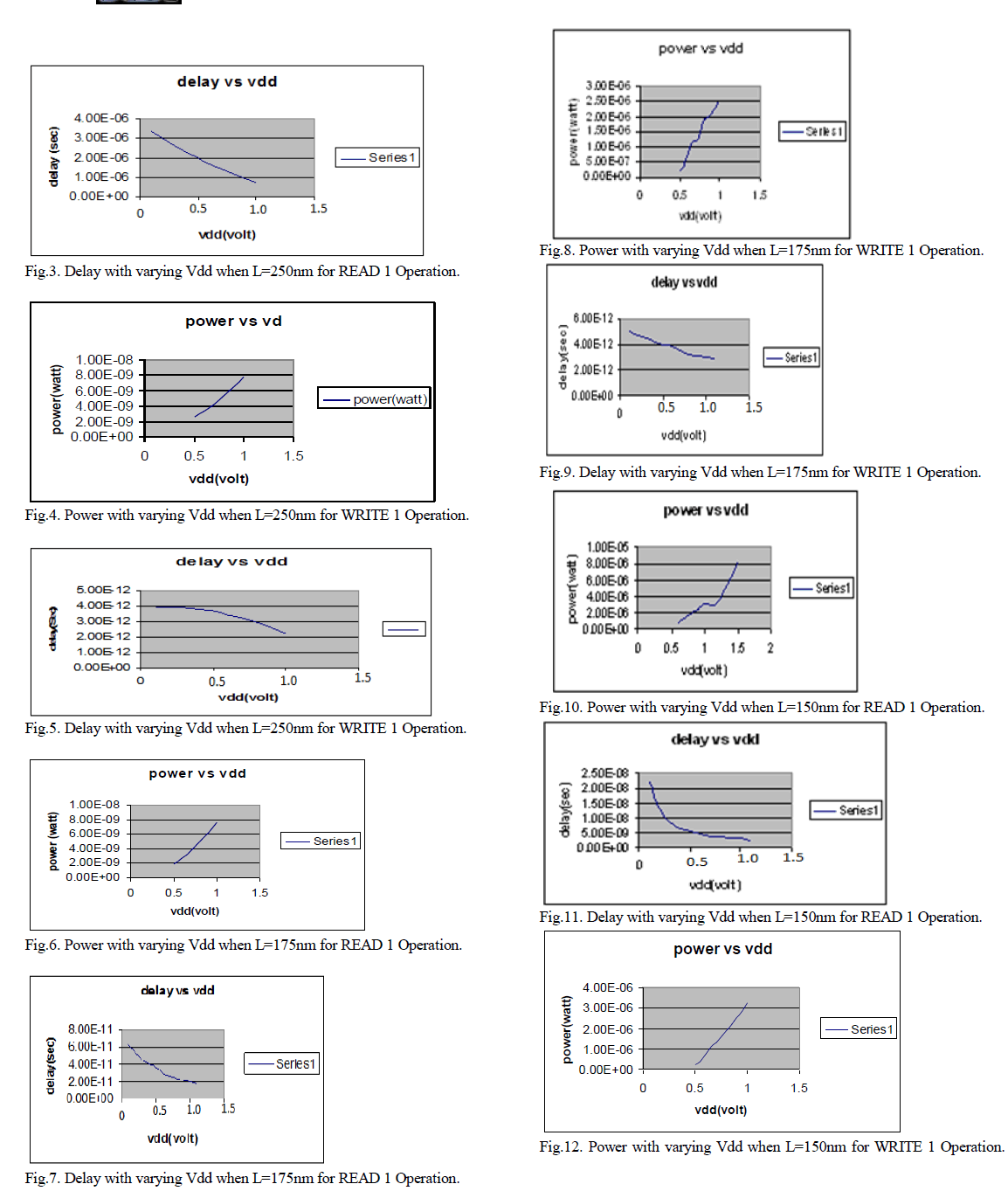
| During write-1 operation as there is only one transistor operating while writing ‘one’ into the cell, so delay is less. |
B. Delay for ‘READ-1’opeartion |
| During read-1 operation as there are two transistors operating while reading one from the cell, so delay is more compare to write one operation. |
| Comparative Power and Delay analysis with Different Channel length MOSFET with different Vdd is described in Table I: |
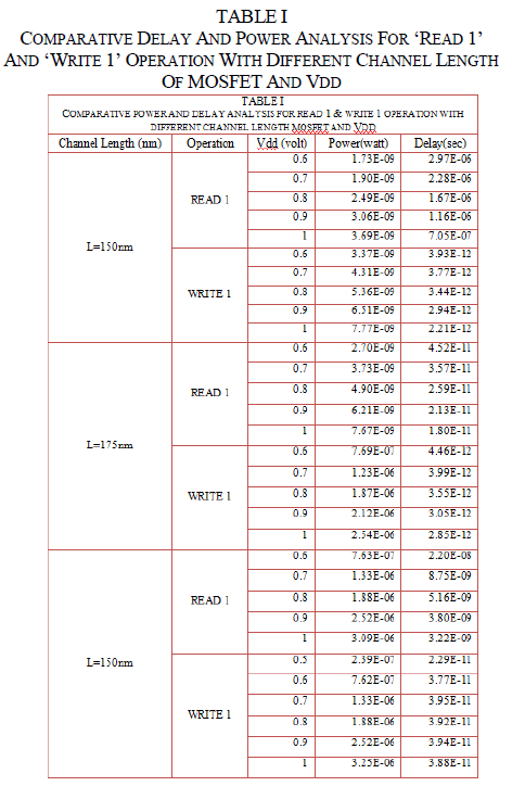 |
 |
 |
IV. RESULT ANALYSIS |
| In this paper, we described the simulated result of 3T DRAM cell, and from the results which we have given in TABLE I, we have observed that: During WRITE-1 operation as there is only one transistor operating while writing ‘one’ into the cell, so delay is less. During READ-1 operation as there are two transistors operating while reading ‘one’ from the cell, so delay is more compare to write one operation. We also observed that when we have varied Vdd from 1 volt to 0.5 volt, the power gradually decreased, and the delay is gradually increased. As we have varied the channel length from 250nm to 150nm, the power has decreased. |
V. CONCLUSION |
| In our work we have varied values of VDD from 1 volt to 0.5 volt. At the same time we have observed the power and delay output for channel lengths 250nm, 175nm, and 150nm with varying VDD. During this work we have observed that power consumption gradually decreases with decreasing values of VDD. Even power consumption decreases with decreasing channel length values. But delay increases with decreasing VDD values. Now while designing a circuit we have to keep in mind that power consumption, delay and cost should be minimum. From the theory, it is clear that power consumption and delay of DRAM cell is not only dependent on VDD but also on load capacitance (Cload), threshold voltage (Vth), and oxide thickness. Therefore for better performance of the device in nano range optimization is needed. |
ACKNOWLEDGMENT |
| The authors would like to thank Prof. (Dr.) M.R.Kanjilal and Faculty Members, Department of Electronics and Communication Engineering, Narula Institute of Technology, WBUT, for many insightful discussions. |
References |
|