International Journal of Advanced Research in Electrical, Electronics and Instrumentation Engineering
ISSN ONLINE(2278-8875) PRINT (2320-3765)
ISSN ONLINE(2278-8875) PRINT (2320-3765)
Shilpa Rao1, Arati.S.Phadke2
|
| Related article at Pubmed, Scholar Google |
Visit for more related articles at International Journal of Advanced Research in Electrical, Electronics and Instrumentation Engineering
With the growing imbalance between processor and memory performance it becomes more and more important to optimize the memory controller features to obtain the maximum possible performance out of the memory subsystem. As system bandwidths continue to increase, memory technologies have been optimized for higher speeds and performance. Improvements in memory latency and bandwidth have not kept pace with reductions in execution time of the instruction. Caches have been used extensively to compensate this mismatch, but some applications do not use caches effectively. As a result, the memory access time has been a hurdle which limits the performance of the system. The problem can be handled by designing a Memory Controller. This paper revolves around implementing and testing the Advanced Microcontroller Bus Architecture (AMBA) compliant Memory Controller as an Advanced Highperformance Bus (AHB) slave. The whole design is captured using Verilog, configured to a FPGA target device belonging to the Spartan 3A and Spartan 3AN family using Xilinx compiler, and simulated with ModelSim. The resulting bit file after compiling is then downloaded to a TKB3S board. The FPGA board is connected to the ADM’s LG320/LGLITE Integrated Logic Analyser and Pattern Generator for testing and verifying the design.
Keywords |
| AMBA specification, AHB slave, Memory Controller, Verilog |
INTRODUCTION |
| Since 1980s, microprocessor performance has improved at a rate of 60% per year. In contrast, latencies have improved by only 7% per year, and bandwidths by only 15-20% per year. The result is that the relative performance impact of memory accesses continues to grow. In addition, the demand for memory bandwidth has increased proportionately (and possibly even super linearly). These trends make it increasingly hard to make effective use of the tremendous processing power of modern microprocessors. |
| Hence, Memory Controllers are built to attack these disadvantages. It provides a high bandwidth and low latency access to off-chip memory. A Memory Controller is a digital circuit which manages the flow of data going to and from the main memory. It can be a separate chip or can be integrated into the system chipset. The front end of the general memory controller buffers requests and responses and provides an interface to the rest of the system. The back end provides an interface towards the target memory. |
| AMBA is an open specification that specifies a strategy on the management of the functional blocks that sort system on chip (SoC) architecture [6]. It is a high-speed, high-bandwidth bus that supports multi master bus management to get the most out of system performance. AMBA specifications are able to maximize the use of system bus bandwidth during dead time. The AHB acts as the high-performance system backbone bus. AHB supports the efficient connection of processors, on-chip memories and off-chip external memory interfaces with low-power peripheral macrocell functions. AHB is also specified to ensure ease of use in an efficient design flow using synthesis and automated test techniques[2]. |
| The memory controller is compatible with Advanced High-performance Bus (AHB), and hence called as “AHB-MC”. It is developed, tested, and licensed by ARM Limited. The list of deliverables in an AHB-MC are as follows: |
| Adheres to the AMBA AHB protocol |
| Availability of synthesis scripts and timing constraints documents |
| Synthesizable VHDL/Verilog RTL source |
| Supports multiple memory devices of different types like SRAM, ROM, and Flash |
| Provides test bench and verification vectors. |
ARCHITECTURE OF AMBA-AHB |
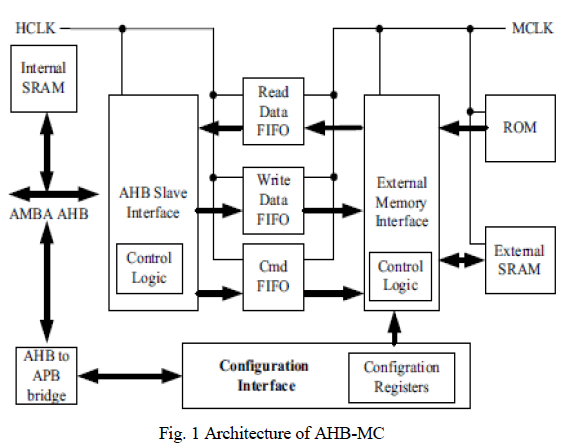
| The AHB-MC mainly consists of five modules: AHB slave interface, configuration interface, external memory interface, memory system, and data buffers [1]. Fig. 1, shows the architecture of AHB-MC. |
 |
A. AHB Slave Interface |
| The AHB slave interface [4] converts the incoming AHB transfers to the protocol used internally by the AHB-MC. Because of the design of the internal inter-connect, some optimizations are made in the interface to improve performance. It is a fully validated component which ensures that it obeys both the AHB protocol and the internal protocol that the interconnect uses. |
B. Configuration Interface |
| The internal memory controller has an APB configuration port. The AHB configuration port is mapped to it using an AHB to APB bridge. The main function of the configuration interface is to change the certain configuration registers according to the commands from AHB to APB bridge which converts AHB transfers from the configuration port to the APB transfers that the configuration interface [3] require. It also provides the read and write enable signals to the data buffers. |
C. External Memory Interface |
| The external memory [4] issues commands to the memory from the command FIFO, and controls the cycle timings of these commands. It generates the 1) Memory bank select and 2) Memory write control signals. |
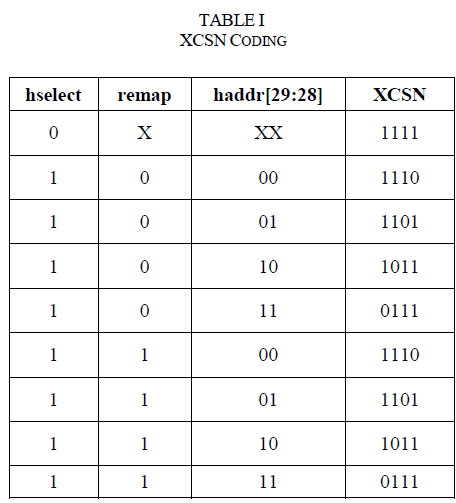
1) Memory Bank Select |
| AHB-MC has four memory banks, which are selected by XCSN signal. The XCSN chip select signal is controlled by the address of a valid transfer, and the system memory map mode. Since, the system will change the memory map after the system boot, the AHB-MC is designed to support a remap signal which is used to provide a different memory map [7]. So before the system memory is remapped, the boot ROM at 0x3000 0000 is also mapped to the base address of 0x0000 0000. The relationship between the inputs and the generated value of XCSN [4] is shown in Table I. |
 |
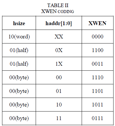
2) Memory write control |
| The external memory controls XWEN for writes in word (32-bit), half-word (16-bit), and byte (8-bit) quantities. The external memory uses hsize[1:0] and haddr[1:0] to select the width and order of each write to memory. Table II shows the relationship between XWEN and the inputs from AHB bus. |
 |
D. Memory System |
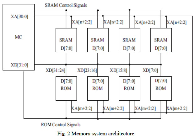
| In the ARM architecture, instructions are all 32-bits, while instructions are 8-bits in the external ROM and SRAM. Therefore the lowest two addresses of ROM and SRAM are not connected to the external address bus. Additionally, to support byte writing, SRAM needs to be separated as four independent banks or has a byte-write enable signal. The basic memory system architecture is shown in Fig. 2. |
 |
| The AHB-MC has two clock domains [3]: AHB clock domain (hclk) and external memory clock domain (mclk). Asynchronous FIFO is used between two clock domains as a data buffer. The main benefit of asynchronous clocking is that the system performance can be maximized, while running the memory interface at a fixed system frequency. Additionally, in sleep-mode situations when the system is not required to do much work, you can lower the frequency to reduce power consumption. |
E. Data Buffers |
| One of the most popular methods of passing data between clock domains is to use a FIFO [5]. A dual port memory is used for the FIFO storage. One port is controlled by the sender which puts data into the memory as fast as one data word (or one data bit for serial applications) per write clock. The other port is controlled by the receiver, which pulls data out of memory, one data word per read clock. Two control signals are used to indicate if the FIFO is empty, full or partially full. |
SYNTHESIS AND SIMULATION RESULTS |
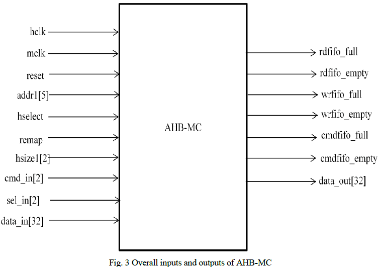
| The architecture of AHB-MC shown in Fig. 1, can be represented in form of a block diagram as shown in Fig. 3. The overall inputs and outputs of the system are also indicated. |
 |
| The functionality of the modules of AHB-MC is tested using Xilinx ISE 10.1 tool in Verilog and simulated using ModelSim 6.2. The following steps are followed during the implementation of this design: Code generation, Simulation, Synthesis, Power analysis, RTL schematic, Translate, Map, Place and Route, and finally Configured to a target device xc3s50a-4-tq144. |
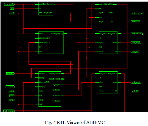
| The RTL Viewer of the AHB-MC is shown in Fig. 4. From this figure, it can be observed that asynchronous FIFOs are used between two clock domains as data buffers. |
 |
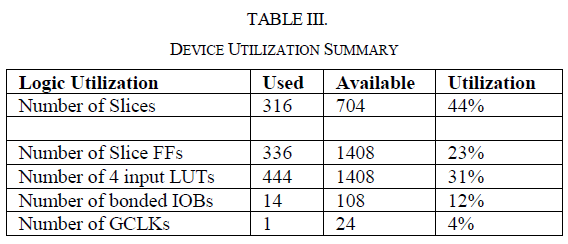
| For a target device XC3S50A belonging to the Spartan 3A and Spartan 3AN family the Device Utilization Summary is shown in Table III. |
 |
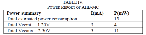
| Power analysis of AHB-MC was carried out by using Xilinx’s XPower Analyzer. Table IV which shows the Power report indicates that the total power dissipated by the AHB - MC is 15mW. |
 |
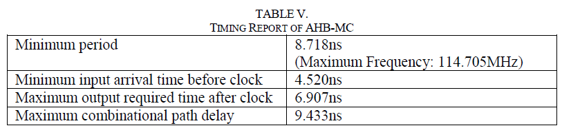
| Timing Summary of the device with Speed Grade -4 is shown in Table V. |
 |
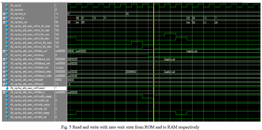
| Fig. 5, shows the simulated waveform which emphasizes read with zero wait states from the ROM. The cmd_in (10- which indicates the ROM read operation) is registered at falling edge of clk (AHB bus clock), after which rd_fifo_rden (Read FIFO read enable) signal goes high. The read data then reaches data_out (AHB data bus) at falling edge of the clk. Write with zero states to the external RAM is also shown in Fig. 5. A write operation to RAM is initiated when cmd_is set to 00. Then the address is send to AHB address bus and wr_fifo_rden (Write FIFO read enable) signal goes high to enable the data from data_in (AHB input data bus) to be stored in the RAM. The sel_in[2] input ensures that the data_out[32] output is channelized to 8 LED outputs of the TKB3S FPGA board. |
 |
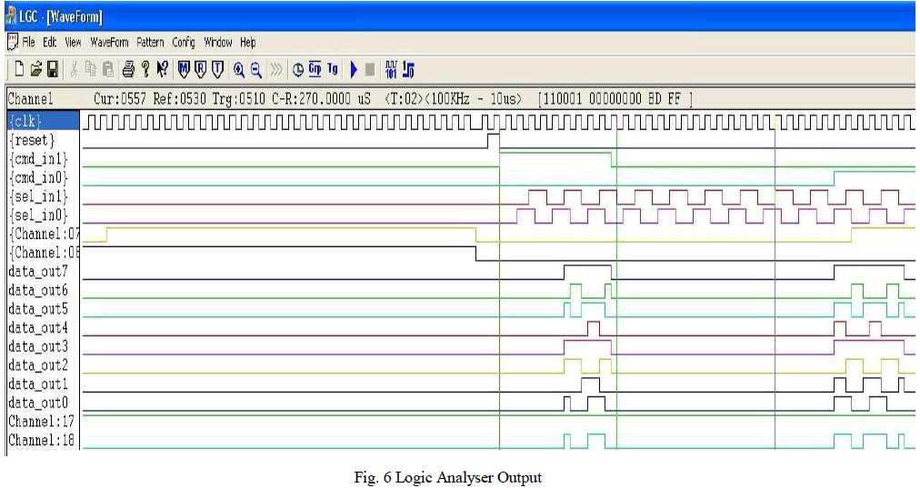
| After RTL Coding and Simulation, Logic Synthesis, Placing and Routing the design, the next step is to test and verify the chip and see if it operates as per the design. Since the design is entirely digital, a testing device ADM’s LG320/LGLITE Integrated Logic Analyser and Pattern Generator is used to test and verify the FPGA target. The Pattern Generator board allows the user to provide custom stimulus (test input) to the Device Under Test (DUT), i.e. xc3s50a-4-tq144 chip. The Logic Analyser board allows the user to analyse the output of the DUT due to the stimulus. |
| Fig. 6, shows the Logic Analyser waveform which indicates that the module operates as per the design. The result i.e. the state or timing data is in a format similar to an oscilloscope display. |
 |
CONCLUSIONS |
| The read write operation is accomplished with zero wait states from the external ROM and the write operation with zero states to the external RAM. |
| With the increase in system frequency, it is hard to achieve address decoding and memory access operations in one clock cycle due to which wait states are inserted. But the method of inserting wait states will result in dramatic drop in system performance. Therefore, the burst method is presented in this paper to resolve the problem. When the first beat of a burst is accepted, it contains data about the remaining beats. For example, when AHB-MC gets the first beat of a read burst, all the data required to complete the transfer can be read from memory and restored in the read data FIFO. So this first transfer has some delay before data is returned. But subsequent beats of the burst can have less delay because the data they require might have already been prepared in the FIFO. |
| Power dissipation is becoming a limiting factor for high performance microprocessor design due to ever increasing device counts and clock rates. The proposed architecture of AHB-MC also aims to optimize power. It is found that it consumes a power of 15mW with a maximum frequency of 114.705MHz. |
| The Logic Analyser and Pattern Generator bundle provides 100 KHz to 100 MHz clock rates for analyzing and debugging the target device. The engineers are provided the ability to leverage the work done during the design phase of the product, simplifying the hardware test environment that provides complete test coverage and excellent debug capability. |
References |
|