International Journal of Advanced Research in Electrical, Electronics and Instrumentation Engineering
ISSN ONLINE(2278-8875) PRINT (2320-3765)
ISSN ONLINE(2278-8875) PRINT (2320-3765)
Rashmi Patil1, Dr.M.T.Kolte2
|
| Related article at Pubmed, Scholar Google |
Visit for more related articles at International Journal of Advanced Research in Electrical, Electronics and Instrumentation Engineering
Digital Signal processing ranks among the most demanding applications of digital design concepts. It is a mature technology domain wherein the demands for enhanced performance and resource utilization have risen exponentially over the years. Finite impulse response (FIR) filters are used in Digital Signal Processing applications.Accuracy in Filter Designing is based on the Multiplication and accumulation of filter coefficients. This paper describes an approach to the VLSI implementation of digital filter which is flexible and provides superior to traditional approaches,low power, and area efficient Discrete Wavelet Transform architecture.
Keywords |
| Adder,Digital signal processing (DSP), finite impulse response (FIR) filter, Multiplier, six tap Fir Filter, VLSI design |
INTRODUCTION |
| With the growing demand on battery powered mobile computing and communication devices, how to achieve low power dissipation in order to extend battery life becomes a major concern of IC designer. DSP systems are widely used in commuting and communication area. FIR filter is one of the basic element in DSP application. Impulse response can either finite or infinite. The method for designing and implementing these two filter classes differ considerably. FIR filters are digital filter whose response to the unit filter (Unit Sample Function) is finite in duration. This is in contrast to Infinite impulse response (IIR) filters whose response to unit impulse is infinite in duration [1]. |
| FIR and IIR filters each have advantages and disadvantage, and neither is based in all situations. FIR filter can be implemented using either recursive or non-recursive techniques, but usually non recursive technique are used. FIR filters are widely used in DSP systems that are characterized by the extensive sequence of multiplications operations. In some applications, the FIR filter circuit must be able to operate at high sample rates, while in other applications, the FIR filter circuit must be a low power circuit operating at moderate sample rates [3],[4]. |
| Filter Unit is a very important unit in every Discrete Wavelet Transform (DWT) architecture. The rest of the paper is organized as follows. Section two and Section three briefly describes Literature review and Discrete Wavelet Transform. Section four presents Data Dependencies within DWT. Proposed Filter Unit and its Filter cell is described in Section five. Section six presents the Hardware Implementation of Filter Unit. Simulation results are shown in Section seven and conclusions are drawn in Section eight. |
II.LITERATURE REVIEW |
| Design of low power, high throughput FIR filter is hot topic in DSP research area. In recent years various technique for low area, low power FIR design have been proposed [1-2]. Bhardwaj et al., [3] introduce the new measurement, power awareness to indicate the ability of the system energy to scale with changing conditions and quality requirements. Parallel (or block) processing can be applied to digital FIR filters to either increase the effective throughput or reduce the power consumptions of the original filters. While sequential FIR filter implementation has been given extensive configuration that deals with directly reducing the hardware complexity or power consumptions of parallel FIR filters [4]. Selecting multiplier with more hardware breadth rather than death would not only reduce the delay, but also the total power consumptions [5]. There is a novel approach for a design method of low power digital base band processing to optimize the bit-width of each filter coefficients [7]. Data transitions power diminution techniques (DPDT) is also used to reduce dynamic switching power of FIR filter [8]. |
| Multiplier plays an important part in today’s DSP systems. Examples of their use occur in implementation of recursive and transverse filters, Discrete Fourier transform, correlation, range measurement and most of these cases it is enough with a multiplier unit design for specific purpose. Multiplier has a large area, long latency and consumes considerable power. The primary objective is power reduction with small area and delay overhead. By using new coding or architectures, it is even possible to achieve both power reduction and area/delay reduction which is strength of high level optimization. In this paper, a novel method to design FIR filter is proposed. Based on pipelining multipliers and adders a very high throughput is achieved. |
III.DISCRETE WAVELET TRANSFORM |
| Wavelet is a small wave whose energy is concentrated in time.Properties of waveletsallow both time and frequency analysis of signals.DWT which is based onsub band coding,is fastcomputation wavelet transform.It is easy to implement and reduces the computation time and resources required.In the case of DWT, a time scale representationof the digital signal is obtained using digital filtering techniques.Thesignalto be analyzed is passedthrough filters with different cutoff frequenciesat different scales. |
| Wavelets can be realized by iteration of filters with scaling.The resolution of the signal,which is a measure of the amount of detail information in the signal,is determined by the filtering operations, and the scaleis determined by upsampling and down sampling (subsampling) operations [2]. |
| A schematic of three stage DWT decomposition is shown in Figure1. |
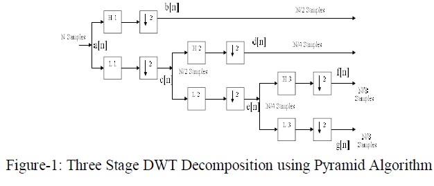 |
| In Figure 1, the signal is denoted by the sequence a[n],where n isan integer. The low pass filter is denoted by L1 while the high pass filter is denoted by H1. At eachlevel,the high pass filter produces detail information b[n], while the low passfilterassociated with scaling function produces coarse approximation;c[n].Here the input signal a[n] has N samples.At the first decomposition level,the signal is passed through the high pass and low pass filters,followed by sub sampling by 2.The output of the high pass filter has N/2 samples and b[n].These N/2 samples constitute the first level of DWT coefficients.The output of the low pass filter also has N/2 samples and c[n]. The signal is then passed through low pass and high pass filters for furtherdecomposition. The output of the second low pass filter followed bysub sampling has N/4 samples and e[n].The output of the second high pass filter followed by subsampling has N/4 samples and d[n].The second high pass filterconstitutes the second level ofDWT coefficients.The low pass filter output is then filtered once again for further decomposition and produces g[n],f[n] with N/8 samples.The filtering and decimation process is continued until the desired levelis reached.The maximum number of levels depends on the length of the signal. |
IV. DATA DEPENDANCIES WITHIN DWT |
| The wavelet decomposition of a 1-D input signal for three stages is shown in Figure 1. The transfer functions of the sixth order high pass (g(n)) and low pass h(n)) filter can be expressed as follows: |
 |
V. THE FILTER UNIT (FU) |
| The filter unit proposed for this architecture is a six-stage non-recursive FIR digitalfilter whose transfer functions for the high-pass andlow-pass components are shown in Equations 2a-2n. |
| FIR filters have the followingadvantages: |
| ïÃâ÷ They can have an exact linear phase. |
| ïÃâ÷ They are always stable. |
| ïÃâ÷ The design method is generally linear. |
| ïÃâ÷ They can berealized efficiently in hardware. |
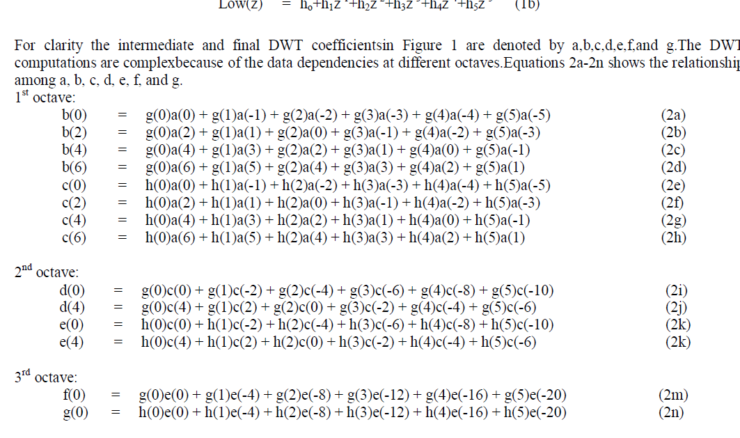
| The latency of each filter stage is1.The systolic architecture of a six-stage filter is shown in Figure 2. |
 |
A. Filter Cell |
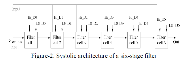
| Equations 1a-1b shows that except for different values of filter coefficients high pass and low pass computations at specific time instants are identical. By introducing additional control circuitry, both computations can perform by the same hardware. Each multiplication must be executed in one clock cycle. The high pass coefficient calculation is performed during the clock cycle when selects ‘0’, whereas the low pass coefficient calculation is performed during the clock cycle when selects ‘1’.The partial results are passed synchronously in a systolic manner from one cell to the adjacent cell. The filter cell consist therefore of only one multiplier, one adder and two registers to store high pass and low pass coefficients. Insuch type of filter cell signed number multiplication problems are occurred. The signed-number represents either positive, negative numbers or one positive and other negative numbers. To avoid this problem, the proposed filter cell consists of invert and xor operation as shown in Figure 3. |
 |
| The filter cell consists of following devices: |
| ïÃâ÷ Multiplier |
| ïÃâ÷ Multiplexer |
| ïÃâ÷ Comparator |
| ïÃâ÷ Adder |
| ïÃâ÷ Not and Xorgate |
VI. HARDWARE IMPLEMENTATION OF FILTER UNIT |
| The filter behaves in a systolic manner by computing partial products of more than one coefficient at a time. The first multiply and accumulate stage computes the first partial product and passes it to the second filter stage where it is added to the second partial product. That repetitive action continues until a complete DWT coefficient is out from the sixth filter stage. The delay through each filter stage is 1 clock cycle. Due to parallel computation of more than one DWT coefficient, the time necessary to complete the computation of the first coefficient in 5 clock cycles. Subsequent coefficients are output every clock cycle. |
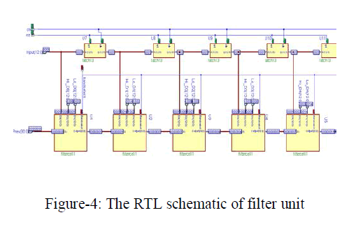
| The filter consists of band select signal. If band selects is’1’ then it selects low pass coefficients. If band selects’0’then it selects high pass coefficients. The filter is controlled by a clock and responds to its high and low levels for the computation of the high-pass and the low-pass DWT coefficient respectively. The RTL schematic of filter unit is shown in Figure 4. |
 |
A. Filter Cell |
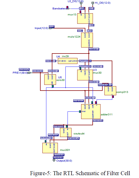
| MATLAB is the software which is used in our project to verify the result with VHDL simulation. The high pass and low pass coefficients are calculated from MATLAB which arein decimal form.Weconvert these into binary and padding some zeroes in it.Because the filter cell and multiplexer is designed for31 bit, 13 bit respectively.Out of this13 bit, 12 bits are data bits and 1 MSB bit is signed bit.The signed bit represents the positive or negative number. |
| The high pass and low pass coefficients are applied to the multiplexer. The multiplexer is used to select the high pass and low pass coefficients. By selecting the particular band, multiplexer selects either high pass or low pass coefficients. Figure 6 shows the RTL schematic of filter cell when band select is high. From 0014 and 1002 it selects low pass coefficients i.e. 1002. |
| The multiplexer performs the multiplication of 1002 and input coefficients; 0009.The output of switches is the input for each filter cell.0009 is the output of one of the switch. This multiplier produces the result is 40000012. The result of multiplier is 31 bit. Here multiplier performs the multiplication of 12 bit only. Remaining MSB bit of 1002 and 0009 perform xor operation. Xor operation is used for signed bit representation. By inserting 6 zeroes, the result of multiplier is 31 bit. |
| The MSB bit of multiplier mul1224 and previous input get xored for addition or subtraction. In xor operation if both the MSB bits are high or low, then the output of xor operation is zero. If one of theinput is low then it produces one output. Here both the MSB bits of 40000042 and 40000012 are one. Hence the output of xor which is ‘sadd’ represents 0 bit. This sad is the selects line for mux301, mux 30 and is added in adder31. |
| The output of multiplier is inverted by using inverter inv29 which is 2FFFFFED. Mux30 select one of the input coming from multiplier is 400000012 and inverter is 3FFFFFED. The select line is zero so it selects 40000012. The comparatorcomp313 compares the previous input and the output of multiplier. It compares 40000042 and 40000012 and displays the result of greater number in the form of MSB bit. Here it represents ‘s’. Adder311 add the previous input, output of mux30 and sadd. The output of comparator is assign to the adder output as a MSB bit. It adds 40000042, 40000012 and 0. The result of adder is 40000054. |
| If carry is generated in adder then it directly displays the result of adder. But if carry is zero then it performs the 2’s complement. Here Cout=Cin=0, then 2’s complement of40000054 is 7FFFFFAC. If select line of mux301 is zero then it selects adder output otherwise it selects the result of 2’s complement. Here the select line is zero, so the final output of filter is 40000054. Initially previous input is 00000000. After applying the clock the control unit uses state diagram. Switches are controlled by using control logic. The output of switch is applied to filter input. |
| The output of first filter cell the previous input for second filter cell and so on. This process is continuous until the complete DWT coefficient is out from six filter stage.The RTL Schematic of Filter Cell is shown in Figure 5. |
 |
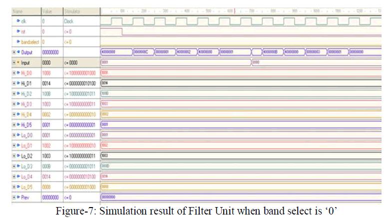
VII. SIMULATION RESULTS OF FILTER UNIT |
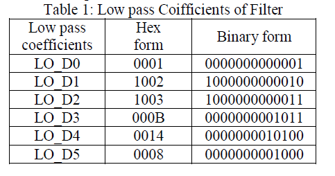
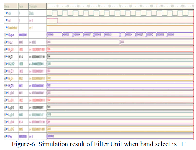
| Simulated waveform for filter unit is as shown in Figure 6 and Figure 7 for different band select. The high pass and low pass coifficients are applied to the filter cell and output is observed from simulated vector waveform. Figure 6 shows waveform for band select ‘1’. At that time low pass coifficients are select as shown in Table 1. |
 |
 |
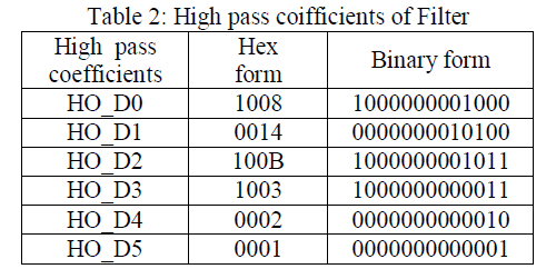
| Figure 7 shows waveform for bandselect’0’.At that time high pass coifficients are select and gives the output. The high pass coifficients are shown in Table 2. |
 |
 |
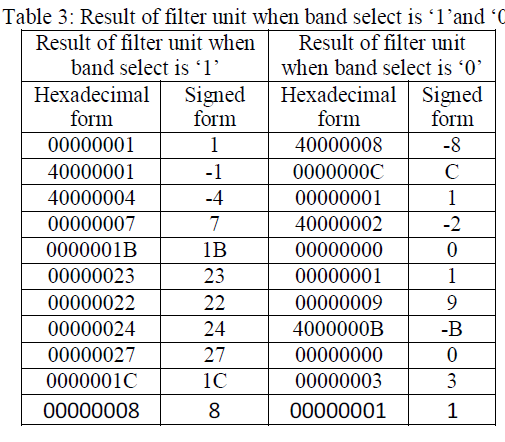
| Table 3 shows the Result of filter unit when band select is ‘1’ and ‘0’. |
 |
VIII. CONCLUSION |
| Design of six-stage non-recursive FIR digital filter for Discrete Wavelet Transform has been presented in this paper. The high pass and low pass coefficients calculation is done in MATLAB. Active-HDL tool is an integrated environment designed for development of VHDL. All the implementation and simulation is done in Active HDL7.1. The VHDL code is compiled and tested. There is no need for complex control circuitry to put the intermediate products in and out of the memory as filter unit is controlled by a global clock. |
References |
|