Keywords
|
| Application-specific integrated circuit (ASIC), area-efficient, CSLA, low delay. |
INTRODUCTION
|
| Design of area- and power-efficient high-speed data path logic systems are one of the most substantial areas of research to perform arithmetic operations in VLSI design there is a scope for reducing area and delay. There is a scope of CSLA in VLSI system design. In digital adders, the speed of addition is limited by the time required to propagate a carry through the adder. The sum for each bit position in an elementary adder is generated sequentially only after the previous bit position has been summed and a carry propagated into the next position. The circuit architecture is simple and area-efficient. However, the computation speed is slow because each full-adder can only start operation till the previous carry-out signal is ready. |
| On the other hand, Carry Look-ahead Adders (CSLAs) are the fastest adders, but they are the worst from the area point of view. Carry Select Adders have been considered as a compromise solution between RCAs and CSLAs because they offer a good tradeoff between the compact area of RCAs and the short delay of CSLAs. Reduced area and high speed data path logic systems are the main areas of research in VLSI system design. High speed addition and multiplication has always been a fundamental requirement of high-performance processors and systems. The sum for each bit position in an elementary adder is generated sequentially only after the previous bit position has been summed and a carry propagated into the next position. There are many types of adder designs available (Ripple Carry Adder, Carry Look Ahead Adder, Carry Save Adder, Carry Skip Adder) which have its own advantages and disadvantages. The major speed limitation in any adder is in the production of carries and many authors considered the addition problem. |
| To solve the carry propagation delay CSLA is developed which drastically reduces the area and delay to a great extent. |
| The CSLA is used in many computational systems design to moderate the problem of carry propagation delay by independently generating multiple carries and then select a carry to generate the sum. It uses independent ripple carry adders (for Cin=0 and Cin=1) to generate the resultant sum. However, the Regular CSLA is not area and speed efficient because it uses multiple pairs of Ripple Carry Adders (RCA) to generate partial sum and carry by considering carry input. The final sum and carry are selected by the multiplexers (mux). Due to the use of two independent RCA the area will increase which leads an increase in delay. To overcome the above problem, the basic idea of the proposed work is to use n-bit binary to excess-1 code converters (BEC) to improve the speed of addition. This logic can be replaced in RCA for Cin=1 to further improves the speed and thus reduces the delay. Using Binary to Excess-1 Converter (BEC) instead of RCA in the regular CSLA will achieve lower area, delay which speeds up the addition operation. The main advantage of this BEC logic comes from the lesser number of logic gates than the Full Adder (FA) structure because the number of gates used will be decreased. This work in brief is structured as follows. Section II deals with the delay and area evaluation methodology of the basic adder blocks and its corresponding delay and area values. Section III deals with the structure and function of BEC logic and its corresponding function table and logic equations. Section IV presents the architecture of the Regular CSLA of 128-bits. This SQRT CSLA has been developed using ripple carry adders and multiplexers. The architecture of the Modified SQRT CSLA is presented in Sections V. In section VI implementation methodologies and corresponding design tools are explained and finally the paper is concluded in section VIII. |
BASIC ADDER BLOCKS
|
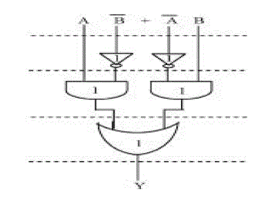
| In this section we explained how to calculate delay and area theoretically. The AND, OR, and Inverter (AOI) implementation of an XOR gate is shown in Fig. 1. The gates between the dotted lines are performing the operations in parallel and the numeric representation of each gate indicates the delay contributed by that gate. Basic adder block considers all gates to be made up of AND, OR, and Inverter, each having delay equal to 1 unit and area equal to 1 unit. We then add up the number of gates in the longest path of a logic block that contributes to the maximum delay. |
| The area evaluation is done by counting the total number of AOI gates required for each logic block. Based on this approach, the CSLA adder blocks of 2:1 mux, Half Adder (HA), and FA are evaluated and listed in Table I. |
INTRODUCTION TO BEC
|
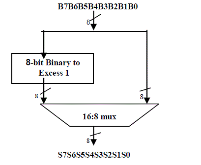
| As stated above the main idea of this work is to use BEC instead of the RCA with Cin=1 in order to reduce the area and power consumption of the regular CSLA. To replace the n-bit RCA, an n + 1-bit BEC is required. A structure and the function table of a 2-b BEC are shown in Fig. 5 and Table II, respectively. Fig.2 illustrates how the basic function of the CSLA is obtained by using the 4-bit BEC together with the mux. |
| One input of the 16:8 mux gets as it input and another input of the mux is the BEC output. This produces the two possible partial results in parallel and the mux is used to select either the BEC output or the direct inputs according to the control signal Cin. |
| as (note the functional symbols ~ NOT, & AND,XOR).The Boolean expression of 8-bit BEC is |
| X0 = ~B0 |
| X1 = B0^B1 |
| X2 = B2^ (B0 & B1) |
| X3 = B3^ (B0 & B1 & B2) |
| X4 = B4^ (B0 & B1 & B2 & B3) |
| X5 = B5^ (B0 & B1 & B2 & B3 & B4). |
| X6 = B6^ (B0 & B1 & B2 & B3 & B4 & B5). |
| X7 = B^ (B0 & B1 & B2 & B3 & B4 & B5 & B6). |
ARCHITECTURE OF 128 BIT CSLA
|
| A 16-bit carry select adder can be developed in two different sizes namely uniform block size and variable block size. Similarly a 32, 64 and 128-bit can also be developed in two modes of different block sizes. Ripple-carry adders are the simplest and most compact full adders, but their performance is limited by a carry that must propagate from the leastsignificant bit to the most-significant bit. The various 16, 32, 64 and 128-bit CSLA can also be developed by using ripple carry adders. The speed of a carry-select adder can be The importance of the BEC logic stems from the large silicon area reduction when the CSLA with large number of bits are designed. The Boolean expressions of the 8-bit BEC is listed improved up to 40% to 90%, by performing the additions in parallel, and reducing the maximum carry delay. |
| The structure of the 128-b regular SQRT CSLA is shown in Fig. 3. It has five groups of different size RCA. The delay and area evaluation of each group are shown in Fig. 3, in which the numerals within specify the delay values, e.g., sum2 requires 10 gate delays. |
MODIFIED ARCHITECTURE OF 128 BIT CSLA
|
| This architecture is similar to regular 64-bit SQRT CSLA, the only change is that, we replace RCA with Cin=1 among the two available RCAs in a group with a BEC. This BEC has a feature that it can perform the similar operation as that of the replaced RCA with Cin=1. Fig 4 shows the Modified block diagram of 64-bit SQRT CSLA. The number of bits required for BEC logic is 1 bit more than the RCA bits. The modified block diagram is also divided into various groups of variable sizes of bits with each group having the ripple carry adders, BEC and corresponding mux. As shown in the Fig.4, Group 0 contain one RCA only which is having input of lower significant bit and carry in bit and produces result of sum[1:0] and carry out which is acting as mux selection line for the next group, similarly the procedure continues for higher groups but they includes BEC logic instead of RCA with Cin=1.Based on the consideration of delay values, the arrival |
COMPARISON OF REGULAR AND MODIFIED128-BIT CSLA
|
| Percentage of delay overhead exhibits a similarly decreasing trend with bit size. The delay overhead for the 8, 16, and 32-b is 14%, 9.8%, and 5.63% respectively, whereas for the 64-b it reduces to only 4.75%. The power–delay product of the proposed 8-b is higher than that of the regular CSLA by 5.2% and the area-delay product is lower by 2.9%. However, the power-delay product of the proposed 16-b CSLA reduces by 1.76% and for the 32-b and 64-b by as much as 8.18%, and 12.28% respectively. Similarly the area-delay product of the proposed design for 16-, 32-, 64-b and 128- b is also reduced by 6.7%, 11%, and 14.4% respectively. |
RESULT
|
| The implemented design in this work has been simulated using Verilog-HDL Modelsim). The adders (of various size 16, 32, 64 and 128) are designed and simulated using Modelsim. All the V files (Regular and Modified) are also simulated in Modelsim and corresponding results are compared. After simulation the different size codes are synthesized using Xilinx ISE 9.2i. The simulated V files are imported into the synthesized tool and corresponding values of delay and area are noted. The synthesized reports contain area and delay values for different sized adders. The similar design flow is followed for both the regular and modified CSLA of different sizes. |
CONCLUSION
|
| A simple approach is proposed in this paper to reduce the area and power of CSLA architecture. The reduced number of gates of this work offers the great advantage in the reduction of area and also the total power. The compared results show that the modified CSLA has a slightly larger delay (only 3.76%), but the area and power of the 64-b modified CSLA are significantly reduced by 17.4% and 15.4% respectively. The power-delay product and also the area-delay product of the proposed design show a decrease for 16-, 32-, and 64-b sizes which indicates the success of the method and not a mere tradeoff of delay for power and area. The modified CSLA architecture is therefore, low area, low power, simple and efficient for VLSI hardware implementation. It would be interesting to test the design of the modified 128-b SQRT CSLA. |
ACKNOWLEDGMENT
|
| G. Omkareswari would like to thank Ms. M.Chitra, Assitant professor ECE Department who had been guiding throughout the project and supporting me in giving technical ideas about the paper and motivating me to complete the work effectively and successfully. |
| |
Tables at a glance
|
|
|
| |
Figures at a glance
|
 |
 |
 |
 |
| Figure 1 |
Figure 2 |
Figure 3 |
Figure 4 |
|
| |
References
|
- O. J. Bedrij, “Carry-select adder,” IRE Trans. Electron. Computes., pp. 340–344, 1962.
- B. Ramkumar, H.M. Kittur, and P. M. Kannan, “ASIC implementation of modified faster carry save adder,” Eur. J. Sci. Res., vol. 42, no. 1, pp.53–58, 2010.
- J. M. Rabaey, Digtal Integrated Circuits—A Design Perspective. Upper Saddle River, NJ: Prentice-Hall, 2001.
- Y. He, C. H. Chang, and J. Gu, “An area efficient 64-bit square root carry-select adder for low power applications,” in Proc. IEEE Int. Symp.Circuits Syst., 2005, vol. 4, pp. 4082–4085.
- Cadence, “Encounter user guide,” Version 6.2.4, March 2008.
|