Keywords
|
| Switch, DAC Logic, CMOS, op-amp, CADENCE, SAR ADC. |
INTRODUCTION
|
| Analog-to-digital (A/D) conversion and digital-to-analog (D/A) conversion, lie at the heart of most modern signal processing systems. As digital signal processing (DSP) integrated circuits become increasingly sophisticated and attain higher operating speeds more processing functions are performed in the digital domain. In most of the electronic systems the input and output signals are analog in nature. Hence, there are analog processing devices like amplifiers as input and output devices. However most of the modifications to be carried out on the input signals before obtaining the outputs are carried out in digital domain. Therefore, there is a need to convert the analog input signals into digital signals at the input end, and after processing them in the digital domain, they have to be converted back into analog signals in most of the applications. The circuits that convert analog signals to digital signals are known as A/D Converters and the circuits that convert digital signals to analog signals are known as D/A Converters. Charge scaling DACs operate by binary dividing of the total charge applied to a capacitor array. This process is implemented by using capacitor to attenuate the reference voltage is shown in Figure 1. Advantage of charge scaling DAC is that it is compatible with switched capacitor circuits [1]. |
| High resolution DACs have been investigated very intensely, due to very high demands for miscellaneous applications such as Analog to Digital Converters (ADC) as well as other industrial applications [2]. Depending on a specific request, many types of high resolution DACs have been introduced [1, 3]. In general they can be classified into two groups: calibrated and non-calibrated DACs. The slower calibrated DACs are using dynamic element matching in order to achieve higher resolutions. On the other hand fast non-calibrated DACs feature, lower resolution as they rely only on matched components. They directly convert any digital code to an analog value. Due to limited matching and linearity performance of the basic device elements, using this kind of converters only up to 12-bit resolution can be achieved. Speed performance in data converters has traditionally been reached with bipolar technologies. However, recent advances in CMOS processes driven by the feature size reduction have led to a considerable improvement in the performance of CMOS devices. Deep sub-micron technologies are expected to improve further, the conversion speed, thus becoming competitive with Bi-CMOS technologies [2]. A new C-2C digital-to-analogue converter (DAC) has been investigated [4], which uses C and 2C capacitors. It is difficult to realize the C-2C DAC scheme on a silicon wafer because of the large parasitic capacitance. The C-2C DACs require considerably less area and power than conventional weighted capacitor (WC) DACs, and operate at a much higher conversion rate. |
| The DAC serves two purposes in a SAR converter: it samples the input charge and it generates an error voltage between the input and current digital estimate [5]. The conventional DAC choice is a binary-weighted capacitor array, which is insensitive to stray capacitance [6]. However, the conventional capacitor array uses charge inefficiently during the conversion. The split capacitor array has both the lowest switching energy and does not require an extra clock phase that would limit high speed operation. |
| The paper is organized as follows: Section I gives an introduction and brief literature survey. Section II deals with the basics of Charge Scaling DAC architecture. Section III details the design of 6-bit Charge Scaling DAC using split array. Section IV presents the design of SAR ADC, Section V gives the simulation results and Section VI conclusions. |
CHARGE SCALING DAC
|
| A very popular DAC architecture used in CMOS technology is the charge-scaling DAC. Shown in Figure 2, a parallel array of binary-weighted capacitors, totaling 2NC, is connected to an op-amp. The value, C, is a unit capacitance of any value. After initially being discharged, the digital signal switches each capacitor to either Vref or ground, causing the output voltage,Vout, to be a function of the voltage division between the capacitors. |
| The capacitor array totals 2NC, therefore, if the MSB is high and the remaining bits are low, then a voltage divider occurs between the MSB capacitor and the rest of the array. The analog output voltage, Vout, becomes as in (1). |
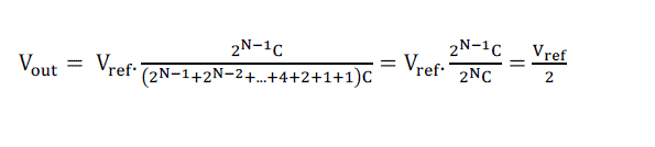 (1) (1) |
| which confirms the fact that the MSB changes the output of a DAC to (Vref/2 ). The ratio between Voutand Vref due to each capacitor can be generalized to, (2). |
 (2) (2) |
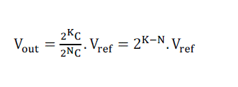
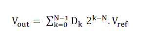
| where it is assumed that the kth bit, Dk, is one and all other bits are zero. Superposition can then be used to find the value of Vout for any digital input word by (3). |
 (3) (3) |
| Two important characteristics of CMOS devices are high noise immunity and low static power consumption. Since one transistor of the pair is always off, the series combination draws significant power only momentarily during switching between on and off states. Consequently, CMOS devices do not produce as much waste heat. CMOS also allows a high density of logic functions on a chip. It was primarily for this reason that CMOS became the most used technology to be implemented in VLSI chips [1]. |
6-BIT CHARGE SCALING DAC USING SPLIT ARRAY
|
| The 6-bit DAC is based on the charge scaling split array method. The block diagram of a 6-bit charge scaling DAC using the spilt array method is shown in Figure 3. This circuit converts a 6-bit digital input word to a respective analog signal by scaling a voltage reference that is obtained by the capacitive network. Various building blocks of Figure 3. are operational amplifier, capacitive network and multiplexer switches to which the digital word is given. Initially the input digital word is given to a multiplexer circuitry. Depending on the logic value of each bit of the word, the multiplexer chooses the particular voltage to which the capacitor is to be charged. If the input bit in the digital word is logic '0' then the multiplexer chooses input which is connected to the 'GND' and the capacitor is charged to 0 V. If the input bit in the digital word is logic '1' then the capacitor is charged to Vref , which is 1.1 V. |
 |
| The capacitor at the end of the network is used as a 'terminating capacitor'. Depending on the capacitors, which are charged to different voltages based on the input digital word, the effective resultant analog voltage is calculated for the respective digital combination. The analog voltage is passed through the op-am and appears as an analog voltage[1]. |
| A. Switch Design |
| A 2:1 multiplexer is very simple to implement in CMOS technology, as only two transmission gates and one inverter are needed. The selection signal (Vin) is used to enable one or the other of the transmission gate switches. When Vin is HIGH, Vhigh is connected to the output Vout . When Vin is LOW, vlow is connected to the output. Figure 4 shows the schematic of 2:1 multiplexer. |
| B. Double Differential Amplifier |
| The differential amplifier is most often used with a current source load as shown in Figure5. If gate voltage of M1 is greater than gate voltage of M2, then drain current of M1 increases with respect to drain current of M2. This increase in drain current of M1 implies an increase in drain currents of M3 and M4. Therefore, the only way to establish circuit equilibrium is for output current to become positive and output voltage Vout to increase. If gate voltage of M1 is less than the gate voltage of M2 then output current become negative and Vout decreases. Biasing is also used for the second structure, with a complementary MOS transistor, which is also driven closely to the corresponding threshold voltage. The extra feature, which is added to the schematic shown in figure 5, to improve the performance of the differential amplifier, is the current mirror at the biasing circuit of the differential amplifier [7]. |
APPLICATION DESIGNED: SAR ADC
|
| The SAR ADC is widely used in many communication systems, such as ultra-wideband and wireless sensor networks which require low-to-medium-resolution converters, with low power consumption. Analog input voltage,Vin, is held on a Sample/Hold device. A SAR ADC architecture is shown in Figure 6. To implement the binary search, N-bit code register in SAR logic block is first set to midscale: N’b100…00, where MSB is logic 1. This forces the DAC output (Vdac ) to be half of the reference voltage (Vref). Then comparator performs a comparison between Vin and Vdac : if Vin is greater than Vdac , the comparator output is a logic HIGH and the MSB of the N-bit code register remains at logic 1, if Vin is less than Vdac , the comparator output is a logic LOW and the MSB of the register cleared to logic 0. The SAR logic then moves to the next bit down, forces that bit HIGH, and does another comparison. The sequence continues all the way down to LSB. Once this is done, the conversion is complete and the N-bit digital word is available in the SAR’s code register [8]. |
| A. Sample and Hold Circuit |
| Sample and hold circuit is used to sample an analog signal and to store its value for length of time. The circuit of sample and hold is shown in Figure 7. The inputs to a sample and hold circuit are sine wave with peak to peak voltage 1.2V and clock signal respectively. During ON period of clock, sampling of input takes place and during OFF period of clock, capacitor holds the sampled value and it is applied to the comparator input. And also during OFF period of clock, conversion from analog to digital takes place. The capacitance of 5pF with initial voltage 0V is taken. |
| B. Dynamic Latched Comparator |
| The dynamic latched comparator is composed of two stages as shown in Figure viii. The first stage is the interfaceintermediate stage which consists of all the transistors except two cross coupled inverters. The second stage is the regenerative stage that is covered of the two cross coupled inverters, where at each stage input is connected to the output of the other. It operates in two phases I) Interface phase and II) Regeneration phase. It has single NMOS tail transistor connected to ground. When clock is low tail transistor is turns off and depending on Vp and Vn output reaches to VDD or ground, if Vp>Vn output of Vp discharge faster than output of Vn. When clock is high (clk = Vdd) tail transistor is turns on and both the outputs discharges to ground [9]. |
| C. Synchronous SAR Control Logic |
| The schematic of the SAR logic consists of shift register and code shift register using D-flip flop as shown in figure ix. Initially the reset line goes low. This line controls set line of FF1 and reset lines of all other sequencer flip flops. |
| The same reset signal also controls the reset line of code register flip flops. Q and Qb of FF1 are set to 1 and 0 respectively. Qb also controls the set line of CF1. Hence the CF1 output is forced to 1. This is the MSB bit and the weight for VFSR/2. It should be noted that since sequence register is reset initially, the set input of all the code registers flip flops except CF1 is logic 1. Hence all the other code register output states are logic0 0. We get a sequence MSB=1 and all other set to 0. The analog equivalent of this weight will be generated by the DAC. When reset goes high and clock is triggered, Q becomes 0 and FF2 outs logic high. This low to high transition of FF2 triggers or clocks the code register flip flop CF1 to store control bus value to its output. When clock runs further, the code register flip flop retains the set value as FF2 output goes to zero. This process is repeated for each of the flip flops until after N clock cycles a high state comes out of sequencer flip flop controlling the code register LSB flip flop [10]. |
SIMULATION RESULTS
|
| All simulations are performed using GPDK 90nm CMOS process technology files in cadence design environment. To design and simulate the charge scaling DAC and its application SAR ADC, Cadence virtuoso schematic editor is used and functionality is verified through simulations using Cadence virtuoso spectre tool. Using cadence virtuoso ADE visualization and analysis XL Browser and XL Calculator, Delay and Power consumption of the overall system is measured. The output waveform of 6-bit charge scaling DAC using split array is shown in Figure 10. Tablle 1 details the simulation results of DAC. A 1.2V, 6-bit SAR ADC and simulated in Cadence Environment. It is observed that, this SAR ADC consumes 802.6μW power. |
CONCLUSION
|
| A 1.1V, 6-bit charge scaling DAC using split array is designed by considering power consumption of the circuit and chip area. Using split method in charge scaling architecture, total area of capacitor is reduced to achieve high resolution of DACs. A 1.1V, 6-bit charge scaling architectures are designed using cadence 90nm technology. The designed 6-bit charge scaling DAC is used in the SAR ADC for the purpose of charge redistribution. A 1.2V, 6-bit SAR ADC is implemented using cadence 90nm technology. |
| |
Tables at a glance
|
 |
| Table 1 |
|
| |
Figures at a glance
|
 |
 |
 |
 |
 |
| Figure 1 |
Figure 2 |
Figure 3 |
Figure 4 |
Figure 5 |
| |
 |
 |
 |
 |
 |
| Figure 6 |
Figure 7 |
Figure 8 |
Figure 9 |
Figure 10 |
|
| |
References
|
- P.E.Allen and Holberg, CMOS Analog Circuit Design, Second Edition, Oxford University Press, 2002..
- V. Liberali, S. Brigati, F. Francesconi, F. Maloberti, “Progress in High-speed and High-Resolution CMOS Data Converters” PROC. 20thInternational Conference on Microelectronics (miel'95), vol 1, nis, serbia, 12-1 4 September, 1995.
- Anshul Agarwal, “Design of Low Power 8-Bit Digital-to-Analog Converter with Good Voltage- Stability”, M.S. Thesis, International Institute ofInformation Technology, Hyderabad 2013.
- S.-W. Lee, H.-J. Chung and C.-H. Han, “C-2C digital-to-analogue converter on Insulator”, Electronic Letters, vol 35, Issue 15, pp 1242-1243.
- Brian P. Ginsburg, Student Member, IEEE, and Anantha P. Chandrakasan, Fellow, “500-MS/s 5-bit ADC in 65-nm CMOS With Split CapacitorArray DAC”, IEEE journal of solid-state circuits, vol. 42, no. 4, april 2007.
- Ashok Srivastava, Siva Yellampalli and Kalyan Golla, “Delta-IDDQ Testing of a CMOS 12-Bit Charge Scaling Digital-to-Analog Converter” ,49th IEEE International Midwest Symposium on Circuits and Systems, 2006 .
- Behzad Razavi, “Design of Analog CMOS Integrated Circuits”, McGraw-Hill International Edition.
- Vijay.V, “Charge Redistribution based 8 bit SAR ADC”, International Journal of Computer Applications 2013.
- Shaik Mastan Vali, Pyla Rajesh, “A 3GHz Low-offset Fully Dynamic Latched Comparator for High-Speed and Low-Power ADCs”,International Journal of Emerging Technology and Advanced Engineering, 2013.
- PEI Xiaomin and zhang,, “Design and Optimization on the Interior DAC of SAR ADC”, ICIME 2011.
|