Keywords
|
| RF Filters; Chebyshev Filters; WLAN Filters; TLY-5A. |
INTRODUCTION
|
| Radio Frequency (RF) and microwave filters were developed since World War II [1]. Thereafter a variety of structure has been demonstrated by researchers in terms of filter compactness and frequency selectivity. Parallel coupled line, comb line, inter digital and hairpin line are significant designs of band pass and band stop filters which shows a good response, however robust and efficient filter structures are need of the hour[2]. |
| Filter plays a significant role in radio frequency and microwave communication systems. Wideband applications requires coupled line microstrip and stripline filters because the demand on selectivity is not severe. On the other hand, wireless applications need miniature filters due to space and cost constraints. There by size reduction has becoming a major consideration for practical application in broadband wireless access communication system. However, the performance of the filter must not be influenced by the reduction in size and the designed compact filter should achieve fine system performances such as good bandwidth, low return loss and accurate centerfrequency [2]. |
| The electrical performances of the filter are described in terms of insertion loss, return loss, frequency selectivity or attenuation at rejection band, group delay variation in the passband. Filters are required to have small insertion loss and large return loss for good impedance matching with interconnecting components, and high frequency selectivity to prevent interference. In mechanical performance aspect, filters are required to have small volume, mass and good temperature stability [2-4]. |
REVIEW OF MINIATURIZED BAND PASS FILTERS
|
| The filter design belong to early time in 1915 when Wagner in Germany and Campbell in the United States came up with an idea of “Electric wave filters” based on lumped approximations to transmission lines. In the 1920s Zobel at Bell Laboratories published a filter design using image parameter technique. Around 1940, Darlington and Cauer extended earlier theories to exactly synthesize network to prescribed transfer functions. Due to the significant computational requirement, these methods remained primarily of academic interest until digital computers were used to synthesize low pass prototype, from which other filter structures were derived. These low pass prototype have been tabulated for many filter transfer functions named after the mathematicians involved in the development of the polynomials, such as Butterworth, Chebyshev, Bessel and others. Thereafter several minimization techniques were proposed by several researches. The minimization is achieved using techniques like spurious response suppression, design using open stub for perturbation for the multimode operation and zero point generation at the stop band control stepped impedance resonators and inter-digital coupling structures, signal interference technique and shape modification using quarter wave stub etc. [1 – 10]. |
DESIGN PERSPECTIVES OF CHEBYSHEV BAND PASS FILTER
|
| Chebyshev filter exhibits a better performance compared to Butterworth filter in terms of frequency response [3-5]. The insertion loss method which is the most commonly used method is adopted in the design as the network synthesis characteristics allows accuracy in frequency response analysis. Fig. 1 represents the process of filter realization. |
| The design starts with the filter specifications and continued with low pass filter prototype that is to normalize in term of impedance and frequency. The low pass filter can be converted into other desired frequency range and impedance level through transformation. Scaling and conversion are used to design high pass, band pass and band stop filter [3]. |
| The design is initiated with a low pass prototype which is a passive, reciprocal low loss two port network, designed to operate from 1Ω generator into a 1Ω load. The filter response has a low pass characteristic with its pass band-edge frequency at ω = 1[3]. |
| The element values for Chebyshev filter with go = 1, ω1 = 1 with a ripple of 0.5dB are shown in Table 1 below. The numbers of orders denoted by N are from 1 to 9 [3]. |
| Scaling and Conversion: For the scaling process we consider scaling of the following parameters namely impedance and frequency scaling. By combining both the impedance and frequency scaling the new element value will be as expressed in (1) and (2). |
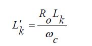 (1) (1) |
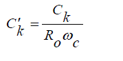 (2) (2) |
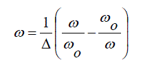
| Conversion: A transformation is required to convert the filter design from the low pass filter to band pass filter. This is achieved by the following conversion. |
 (3) (3) |
| For ω = 1 and ω = -1 to map to ω1 and ω2 then |
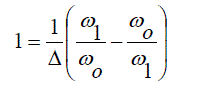 (4) (4) |
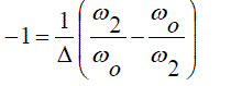 (5) (5) |
| The frequency tends to shift from low pass to band pass as shown in Fig. 2. |
| By applying the transformation to the inductor, the inductor gets converted to series combination of inductor and capacitor and by applying the transformation to the capacitor the capacitors gets converted to parallel combination of inductors and capacitors. |
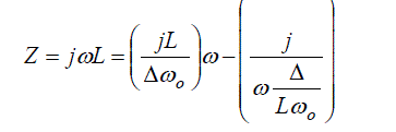 (6) (6) |
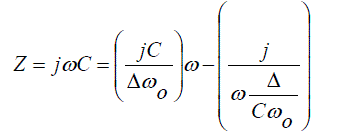 (7) (7) |
| Filter Realization: The filter is realized using microstrip transmission line. Fig. 3 is the basic microstrip parallel coupled line coupler. The characteristic impedance Zo of the micro strip is |
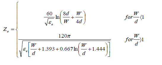 (8) (8) |
| It is easy to fabricate multi-section parallel coupled line band pass in microstrip technology with bandwidth less than that of 20%. As the bandwidth of the filter gets wider, it becomes difficult to fabricate because the coupled line are required to get more closely to each other. Parallel coupled line filter has properties of superposition of even and odd mode excitations [6-8]. |
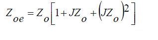
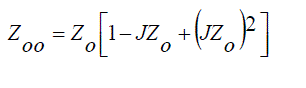
| In order to design a narrow band pass filters, number of coupled line are cascaded as indicated in Fig. 4. Even and old impedances are denoted are ZOe and ZOo respectively. The values of Zo should be around 50Ω since they represent the input and output. Hence they are matched by SMA connectors [8]. |
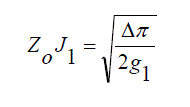 (9) (9) |
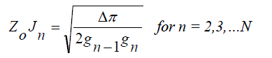 (10) (10) |
 (11) (11) |
 (12) (12) |
DESIGN SPECIFICATIONS
|
| In filter design the most important thing to be considered is the specification such as center frequency, bandwidth, insertion loss, stop band attenuation and the ripple of the desired filter. The filter specifications listed in Table 2 are with reference to the RF filter specifications proposed for WLAN applications [4]. |
| Defined with the specifications of the filter design the order of the filter should be determined. The order of the filter is computed as |
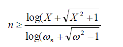 (13) (13) |
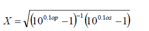 (14) (14) |
| Pass band ripple p= 0.5 dB and the stop band ripple s= 0.25 dB, therefore X = 50.828 and n > 8.55 = 9 |
| The normalized parameter of the 9th order Chebyshev filter lumped elements is then determined based on the element value for ripple low pass filter prototype at 0.5dB ripple. |
| The coupled line are calculated as ZoJ1 = 0.1641, Zoe = 59.5500, Zoo = 43.1422, with the consideration of n = 1 Δ = 0.03 and g1=1.7504 F. And the final values of the even and odd impedance are determined as listed in Table 4. |
RESULTS AND DISCUSSION
|
| A. Conventional 9th Order Chebyshev Band Pass Filter |
| The schematic of the 9th order conventional Chebyshev band pass filter is shown in Fig. 5. The dielectric constant and loss tangent of the structuremodelled using TLY-5A were 2.16 and 0.0009 respectively with a substrate thickness of 0.508mm .Next FR4 was used as a substrate. The dielectric constant and loss tangent of FR4 were 5.2 and 0.019 respectively with a substrate thickness of 1.6mm. |
| The physical length (P) width (W) and separation (S) were determined by simulation using Ansoft Designer SV for TLY-5A and FR4 as stated in Table 5 and 6. |
| Comparing W and S of TLY-5A and FR4 the dimension of FR4 is greater compared to TLY-5A. However if P is compared the FR4 is smaller compared to TLY-5A which eventually makes FR4 smaller in length compared to TLY- 5A. From simulation layout of TLY-5A and FR4 as indicated in Fig. 6 and 7, it is clear that compared to TLY-5A, FR4 is smaller in length whereas the width of separation is greater. |
| Fig. 8 and 9 show the frequency responses for TLY-5A and FR4 respectively. The red color line represents the Return Loss (S11) and the blue line represents the Insertion Loss (S21).Table 7 is the comparative analysis of theoretical and experimental result from Fig. 8 and 9. The insertion loss of the substrate TLY-5A did achieve its expected target with a value of -4.59dB whereas for FR4 the results are nowhere near the target with a value of -37.37dB with a difference of around 27dB. The return loss for TLY-5A did achieve the targeted values; however for FR4 it has not achieved the target. |
| Focusing on bandwidth of the conventional band pass filter designed on substrate TLY-5A is wider than that of the expected results by 65 MHz while the bandwidth of the filter simulated from FR4 is narrower by 8MHz compared to the expected results. |
| After a good observation of the conventional type result, optimization is needed in order to achieve the target values. Optimization is based on parameter study (trial and error method) where the W, S and P parameters are changed until a desired value is yielded. It is advised to change one parameter at a time so that one can notice the effect of each parameter. The FR4 filter needs more optimization since its insertion loss is drifted far away compared to that of TLY- 5A. |
| Table 8 and 9 is the optimized values for both TLY-5A and FR4 substrates. The width, space and physical length of each coupled lines should be approximately the same except for the first and last coupled lines to match the input and output of the Chebyshev band pass filter. This in turn will give rise to the return loss (S11). |
| Fig. 10 is the frequency response of band pass filter of TLY-5A. The insertion loss S21 is -5.97dB whereas the return loss S11 is -15.10dB. The filter operates ata operates at a bandwidth of 100 MHz from 5.7 to 5.8 GHz. The optimization in TLY-5A contributes to target values. |
| Figure 11 is the frequency response for FR4. The insertion loss is -10.95dB. The return loss of the optimized FR4 yielded a value of -11.41dB and the bandwidth is around 463MHz. The Optimization of FR4 seemed to have improved the filter in terms of insertion loss and return loss whereas the bandwidth has increased if compared to the filter before any optimization was done. |
| Table 10 compares the simulated results of both TLY-5A and FR4 with the theoretical values. On comparison, TLY- 5A filter achieves the expected results whereas FR4 is better in terms of insertion loss and return loss after optimization but the bandwidth of the FR4 has increased by 363MHz. |
| Table 11 shows the effects of varying the width W, spacing S and physical length P of each coupled line. The effects were obtained from parameter study of each parameter. Parameter under study is varied while the others are kept constant. |
| B. Λ-type Chebyshev 9th Order Bandpass Filter |
| The proposed Λ type filter minimizes the size of the structure mainly by changing the shape of the parallel coupled lines. Fig. 12 and 13 are the design of the proposed Λ-type Chebyshev 9th order bandpass filter using TLY-5A and FR4 respectively. The Λ type filter exhibits an area reduction of 51 % compared to the conventional filter. |
| Fig. 14 shows the frequency response of Λ-type Chebyshev 9th order bandpass filter for TLY-5A, the insertion loss for the Λ-type bandpass filter design on TLY-5A is -5.97dB and the return loss is -15.10dB at a cut-off frequency 5.75GHz. The bandwidth measured in the range of frequencies between 5.701GHz and 5.803GHz is 102MHz. |
| Fig. 15 is the frequency response of Λ-type Chebyshev 9th order bandpass filter for FR4. The insertion loss (S21) of Λ- type bandpass filter is -10.95dB and the return loss (S11) is -11.45dB at cut-off frequency 5.75GHz. The bandwidth measured is the range of frequency between 5.499GHz and 5.962GHz is 463MHz. |
| Table 12 is the comparison of Λ-type Chebyshev 9th order bandpass filter simulation results. The Λ-type 9th order bandpass filter design on TLY-5A substrate achieves the expectation values whereas for FR4, the bandwidth does not meet the specification. However, the bandwidth of Λ-type bandpass filter designed on FR4 is getting narrower than that of the conventional bandpass filter designed on FR4. |
| Table 13 compares the parameters of for conventional and Λ-type Chebyshev 9th order bandpass filter designed using TLY-5A andFR4. The results of the filter using TLY-5A are approximately the same. On the other hand, the frequency response for Λ-type designed on substrate FR4 is better compared to the conventional as the bandwidth is narrower than the conventional. However the insertion loss decreased by 1.28dB. |
CONCLUSION
|
| The paper has presented a design structure for the reduction of size of the 9th order Chebyshev bandpass filter. The size of the bandpass filter is reduced by 51 % compared to conventional filter. The results also indicate that the filter designed with TLY-5A exhibits a comparable response in comparison with conventional filter. Optimization can be still carried over the improvement of insertion and return loss. |
| |
Tables at a glance
|
 |
|
|
|
|
| Table 1 |
Table 2 |
Table 3 |
Table 4 |
Table 5 |
| |
|
|
|
|
|
| Table 6 |
Table 7 |
Table 8 |
Table 9 |
Table 10 |
| |
|
|
|
| Table 11 |
Table 12 |
Table 13 |
|
| |
Figures at a glance
|
 |
 |
 |
 |
 |
| Figure 1 |
Figure 2 |
Figure 3 |
Figure 4 |
Figure 5 |
| |
 |
 |
 |
 |
 |
| Figure 6 |
Figure 7 |
Figure 8 |
Figure 9 |
Figure 10 |
| |
 |
 |
 |
 |
 |
| Figure 11 |
Figure 12 |
Figure 13 |
Figure 14 |
Figure 15 |
|
| |
References
|
- Mongia, R., Bharita, P., and Bahl, I.J., “RF and Microwave Coupled Line Circuits”, 2nd Ed., Artech House Publishers, 1999.
- Simon, A.E., and Yaw, L.K., “A Modern Bandpass Microstrip Filter With Spurious Response Suppression and Size Reduction”, Asia-PacificConference onApplied Electromagnetics, pp.1-5, 2007.
- Pozar, D.M., “Microwave Engineering” 4th Ed., Wiley and Sons, 2011.
- Othman, A.R., Ibrahim, I.M., Selamat, M., Samingan, M., Aziz, A., and Halim, H. C., “5.75 GHz MicrostripBandpass Filter for ISM Band”,Asia-Pacific Conference on Applied Electromagnetics, pp.6-10, 2007.
- Winder, S., “Filter Design”, 2nd Ed., Reed Educational and Professional Publishing Ltd, 2001.
- Hunter, I.C., “Theory and Design of Microwave Filters”, 2nd Ed., Institution of Engineering and Technology, 2006.
- Alaydrus, M., “Designing Microstrip Bandpass Filter at 3.2 GHz”, International Journal on Electrical Engineering and Informatics, vol. 2, no. 2,
- Moradian, M., and Khalaj-Amirhosseini, M., “Improvement the Characteristics of the Microstrip Parallel Coupled Line Couple by Means ofGrooved Substrate”, Progress in Electromagnetics Research, vol. 3, pp.205-215, 2008.
- Hung, C., Weng, M., Yang, R., andSu, Y., “Design of the Compact Parallel Coupled Wideband Bandpass Filter With Very High Selectivity andWide Stop Band”, IEEE Microwave and Wireless Components Letters, vol.17, no.7, pp.510-512, 2007.
- Liang, C., and Chang, C., “Compact Wideband Bandpass Filters Using Stepped-Impedance Resonators and Interdigital Coupling Structures”,IEEE Microwave and Wireless Components Letters, vol.19, no.9, pp.551-553, 2009.
|