Keywords
|
| Flash ADC, Analog demultiplexing, high-speed comparator, time-domain latch interpolation, Time interleaved ADC |
INTRODUCTION
|
| High speed applications such as 40GbE and 100GbE aiming at high data-rate communications, ADCs for these structures are demanded to have several gigahertz-order sampling rates. One of the recent trends for such high-speed ADC strategy is interleaving low-power SAR ADCs [15]. However, the conversion speed of above ADCs are limited, it is required to use high speed ADCs such as Sigma Delta ADC, Flash ADC etc. |
| This paper presents a 1:16-demultiplexing architecture in 45nm low power CMOS. This architecture used with 16 time interleaved ADCs at the outputs. Thus the sampling rate per channel can be significantly reduced to 2.5 GS/s per sub-ADC compared to 40 GS/s for the whole ADC. |
| Flash ADCs extremely fast compared to many other converters. However, preamplifiers, which are often required to relax the effects of comparator offset and metastability, increase the total power consumption. In addition, the input parasitic capacitance by the preamplifiers still remains a bottleneck for high-speed and low-power operation. One of the popular design techniques for addressing the above problem is the preamplifier interpolation scheme [21]. However, the static power consumption by the remaining preamplifiers is still not desirable given recent low power demand. Although the offset problem can be resolved without preamplifiers by using calibration [15], kickback noise from dynamic latches to the input signal (or sampling circuit) and to the reference ladder may degrade the signal integrity, resulting in SNR degradation. Thus, reduction of the number of dynamic latches will help to enhance the circuit performance by virtue of reduced dynamic noise. Recently, a time-domain latch interpolation technique that reduces the number of first-stage dynamic latches by half [15]. The present paper presents detailed operational principles and design considerations of Time Interleaved Flash ADC and demonstrates with higher operating frequency and better performance. |
| The rest of the paper is organized as follows. Section II describes the complete system architecture. Section III describes time interleaving and analog demultiplexing. Section IV describes the proposed 6-bit flash ADC with time domain interpolation technique. Section V provides the results and section VI concludes this paper. |
SYSTEM ARCHITECTURE
|
| Fig. 1 shows the architecture of the 6-bit 16-way interleaved flash ADC, The architecture consist of an analog demultiplexer followed by sample and hold circuit, 16 six bit flash ADC of 2.5 GS/s and a 16:1 digital multiplexer (TDM). For a good performance of the demultiplexer a highly linear current has to be supplied to the differential input. This is done by transconductance amplifier, which is further explained in section II. The flash ADC implemented in this architecture uses time domain latch interpolation technique, that reduces the number of comparators and hence power conception and die area. The TDM is used for demultiplexing 16 output line produced by the bunch of ADCs to a single channel [19]. Clock generator and delay generator circuit is aimed for creating appropriate clock signal for each element of this architecture. |
ANALOG DEMULTIPLEXING
|
| The theory of the analog demultiplexer (DEMUX) is based on the integration of an input current by means of capacitors, which are connected to the input for a defined time slot. The current is generated by a highly linear transconductance. By simple NMOS-transfer transistors in the DEMUX itself the current is switched stepwise to the 16 outputs. Hence only a very small part of the connected circuits, which may here be considered as load capacitances, have to be reloaded in one sampling time interval. When the signal is completely sampled on the capacitor it is resampled by a Sample-and-Hold (S/H) circuit. This holds the signals constant for the following ADCs, which are by help of this decoupled from changes induced by the demultiplexing or the reset process [22]. |
| Fig. 2 shows the current transmission process for one subchannel of the differential demultiplexer. First the input voltage V is converted to a current I. This is summed up in a time slot T on the respective load capacitance Cs. Afterwards the resulting output voltage is sampled by a S/H. This allows resetting the capacitor during the hold-mode with the switch. |
| For a good performance of the demultiplexer a highly linear current has to be supplied to the differential input. Fig. 3 shows the developed transconductance amplifier. It is linearized with linearization resistors R and the Miller effect is reduced by a cascoded NMOS-pair on top of the input transistors. To further increase the linearity the current source of the amplifier has a value of 3.5 mA, while only Iout,max = 0.75 mA is used to load the capacitors at the end of the demultiplexer chain. The difference is subtracted by two PMOS current sources. This keeps the transistors of Fig- 3 in the same operation regions for the used output current range. The amplifier requires a second lower supply voltage VSS2 of about -2.5 V in addition to the regularly used -1.4 V to ensure a fast and linear operation. |
6 – BIT FLASH ADC
|
| A prototype 6bit flash ADC has been designed to verify the proposed time-domain latch interpolation technique. The structure is shown in Fig. 5. This ADC consists of an input sample and hold circuit (S/H), a resistor ladder, three stages of latches with the proposed latch interpolation, a digital encoder, calibration logic and clock buffers. |
| Traditionally, the most suitable ADC architecture for high speed operation with low-to-medium resolution has been the flash type. However, preamplifiers often required to relax the effect of comparator offset and metastability increase the total power consumption. In addition, the large input parasitic capacitance by the preamplifiers has been a major drawback for high-speed and low-power operation. One of the popular design techniques for the above problem in flash ADCs is the preamplifier interpolation scheme. The technique reduces the number of preamplifiers and generates the missing information by interpolating the outputs of the two adjacent preamplifiers. However, the static power consumption by the preamplifiers, even though the number is reduced, is still the major source of power consumption. Recently, several designs have reported flash ADC structures that have no preamplifiers [4-7]. However, the absence of the preamplifiers makes the flash ADC’s performance to be affected by comparator offset serious. Thus, the preamplifier-less flash ADC often requires complicated offset calibration scheme. In addition, even though the offset problem could be solved in the preamplifierless structure, the kickback noise from the dynamic latch to the input terminal and the reference ladder can seriously degrade the signal integrity, which results in SNR degradation. Thus, reduction of the number of latches will enhance the circuit performance by reducing noise and power reduction. In this paper, motivated by the discussion above, we propose a time-domain latch interpolation technique to reduce the number of dynamic comparators and to take many advantages from it: reduced input capacitance, low power consumption, less kickback noise, and reduced complexity for offset calibration. |
| A. Time-Domain Latch Interpolation |
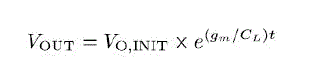
| In order to distinguish the latch used as a comparator from the latch functioning as a pure digital storage element, the latch used for the comparator is hereafter referred to as a dynamic latch. Unlike the preamplifier, the dynamic latch is not a linear circuit for input voltage, because its output eventually reaches a logic high or low level depending only on the input polarity. Thus, linear voltage interpolation using the neighbouring outputs at a steady state is not possible with dynamic latches. Nonetheless, the dynamic latch still shows input dependent nonsaturated behaviour when it performs positive-feedback-based amplification, and, therefore, it is still possible to extract the interpolation information during a limited time period. The output settling behaviour of a dynamic latch that is simply modeled as two cross-coupled inverters can be expressed as an exponential function with a time constant CL/gm [15] as |
 (1) (1) |
| Where VOUT is the output voltage of the latch, VO,INIT is the initial output voltage at the beginning of the latching phase, gm is the transconductance of the inverter that incorporates the latch, and CL is the load capacitance. Equation (1) implies that the output settling behaviour of a dynamic latch (before the output saturates) contains more than binary (low or high) information. A few recent studies showed that a single dynamic latch can achieve a resolution greater than 1 b by relying on this time-related information [22]. However, since these techniques depend on the absolute timing, which is very sensitive to variations such as process, supply voltage, and temperature variations, background calibration must be used to map the timing information to certain voltage level(s). On the contrary, if the relative timing information between the latches can be used for additional information, it will be robust to PVT variations. Fig.4 shows the proposed time-domain latch interpolation technique. Dynamic latches are cascaded to compensate for insufficient latching time, as accomplished in many previous designs [21], and those in the second array (L4 – L6) amplify the outputs of the first-stage dynamic latches. Note that the circuits are drawn in a single-ended version for simplicity. Two dynamic latches L1 and L2 compare the input signal (Vin) with their own references Vref_k and Vref_k+2, and the missing dynamic latch was supposed to compare Vin with Vref_k+1 , where Vref_k+1 is the centre level of Vref_k and Vref_k+2. The missing zero-crossing information by the eliminated dynamic latch is generated (interpolated) by L5 in the second-stage dynamic latch array using two neighbouring signals, Vref_k+ and Vref_k+2. |
| B. Dynamic latch for the 1st stage |
| Fig. 6(a) shows the schematic of the proposed latch for the use of the 1st stage. Compared with the popular conventional structure shown in Fig. 6(b) [23], the proposed latch has an additional NMOS latch to ground path. The additional latch helps for the comparator to turn on fast from the reset phase by discharging the output node faster than the conventional design owing to the reduced number of stack. This also enhances the latching time constant. The latches in 2nd and 3rd stages have the conventional structure shown in Fig. 6(b). This is due to the relaxed latching time constant requirement in them owing to the amplified signal via the 1st stage. Note that the input pair structure is simplified with a single differential pair while the real design for the 1st stage latches and the interpolation latches in the 2nd stage have two differential pairs for input and references. The proposed scheme also has some drawbacks as well. The additional latch increases noise and offset level. This is not only due to the increased number of transistors, but also due to the effective gain reduction. Since the turn-on time of the dynamic latch is shortened due to the signalindependent fast discharge of the output via the additional NMOS latch to the ground, the contribution of the input signal to the output voltage difference is reduced when regeneration begins to dominate [15]. Because of this reduced effective gain, the input referred offset and noise increases. The input referred offset is slightly increased to 12.3 mV from the conventional one’s 10.7 mV. The input referred noise of the proposed dynamic latch is about 1.15 mV while that of the conventional one is approximately 0.85 m. Since the noise voltage corresponds to 0.1 LSB, the increased offset effect to the performance is not considerable. It should be noted that the reduced effective gain discussed here is focused only at the time when the regeneration begins and, therefore, it does not mean slow regeneration speed. As shown in Fig. 7, actual latching speed is enhanced because the total transconductance of the latches is increased due to the increased current through the pMOS and the increased total size of the nMOS. In addition, the regeneration operation begins earlier in the proposed design than it does in the conventional design [11]. |
RESULTS
|
| A 6 bit FLASH ADC was implemented in a 45nm GPDK CMOS technology. The measured peak DNL and INL are 0.53LSB and 0.61LSB, respectively after calibration. Fig 7 shows the transient wave of the dynamic latch which is used in the first stage this work. The measured signal to noise and distortion ratio (SNDR) and spurious free dynamic range (SFDR) are 42.1dB and 33.3dB, respectively. The ADC core consumes 69mW at 1.2V supply. |
CONCLUSION
|
| A 40 GS/s Flash ADC for 40GbE application was implemented on the basis of 1:16 time interleaving technique. Time domain latch implementation of flash ADC is reduced the number of comparators on the first stage and the power conception. The conversion speed of the ADC can be further improved by increasing clock tree size to the Demultiplexer. |
| |
Figures at a glance
|
 |
 |
 |
 |
| Figure 1 |
Figure 2 |
Figure 3 |
Figure 4 |
| |
 |
 |
 |
| Figure 5 |
Figure 6 |
Figure 7 |
|
| |
References
|
- Detlef Daniel,Ulrich Langmann and Berthold G. Bosh, “A Silicon Bipolar 4- bit 1-Gsamples/s Full Nyquist A/D Converter”IEEE J. Solid state circuits, Vol.23 No. 3 pp. 742-749 June 1988
- Mohammed O. Shaker, Soumik Gosh and MAgdy A.Bayoumi, “A 1- GS/s 6-bit Flash ADC in 90nm CMOS” IEEE conferencepp. 144-147 2009
- Vinayashree Hiremath and Saiyu Ren,“An Ultra High speed Encoder for 5GSPS Flash ADC” IEEE custom integrated circuitsconference pp. 1-6, 2010
- Anchada Charoenrook and Mani Soma “A Fault Diagnosis Technique for Flash ADC’s”, IEEE Transactions on circuits andsystems –II Analog and digital signal processing, vol. 43, No 6, pp. 445-457 June 1996
- Steven B. Kaplan, Sergey V. Rylov and Paul D. Bradley “Real Time Digital Error Correction for Flash Analog-To-DigitalConverter” IEEE transactions on applied super conductivity, Vol. 7 No.2 pp. 2822-2825 June 1997
- Ayman Ismail and Mohamed Elmasry, “A 6-Bit 1.6-GS/s Low-Power Wideband Flash ADC Converter in 0.13-μm CMOSTechnology” IEEE J. Solid state circuits, Vol-43 No.9, pp.1982-1990, September 2008
- Shahriar Shahramian, Sorin P. Voinigescu, and Anthony Chan Carusone, “A 35-GS/s, 4-Bit Flash ADC With Active Data andClock Distribution Trees”, IEEE J. Solid state circuits, Vol-44 No.6, pp.1709-1720, June 2009
- Ying-Zu Lin, Cheng-Wu Lin, and Soon-Jyh Chang “A 5-bit 3.2-GS/s Flash ADC With a Digital Offset Calibration Scheme”IEEE Transactions on VLSI systems Vol. 18, No.3 pp. 509-513, March 2010
- Chun-Chieh Chen, Yu-Lun Chung and Chen-I Chiu “6-b 1.6-GS/s Flash ADC with Distributed Track-and-Hold Pre-Comparators in a 0.18μm CMOS” IEEE custom integrated circuits conference pp. 1-4, 2009
- Dharmendra Mani Varma “Reduced Comparator Low power Flash ADC using 35nm CMOS” IEEE custom integrated circuitsconference pp. 385- 388 2011
- Jong-In Kim, Wan Kim, Barosaim Sung, and Seung-Tak Ryu, “A Time-domain Latch Interpolation Technique for Low PowerFlash ADCs” IEEE custom integrated circuits conference, pp.1-4, 2011
- Amol Inamdar, Anubhav Sahu, Jie Ren, Aniruddha Dayalu, and Deepnarayan Gupta, “Flash ADC Comparators and Techniquesfor Their Evaluation” IEEE Transactions on applied super conductivity, Vol.23, No.3, pp. 1400308 June 2013
- Ying-Zu Lin, Chun-Cheng Liu, Guan-Ying Huang, Ya-Ting Shyu, Yen-Ting Liu, and Soon-Jyh Chang, “A 9-Bit 150-MS/sSubrange ADC Based on SAR Architecture in 90-nm CMOS” IEEE transactions on circuits and systems-I Regular papersVol.60, No.3 pp. 570-580 March 2013
- Mohammad Chahardori, Mohammad Sharifkhani, and Sirus Sadughi “A 4-Bit, 1.6 GS/s Low Power Flash ADC, Based onOffset Calibration and Segmentation” IEEE transactions on circuits and systems-I: Regular papers, Vol.60, No.9, pp. 2285-2297, September 2013
- Jong-In Kim, Ba-Ro-Saim Sung, Wan Kim, and Seung-Tak Ryu, “A 6-b 4.1-GS/s Flash ADC With Time-Domain LatchInterpolation in 90-nm CMOS”, IEEE J. Solid state circuits, Vol.48, No 6. pp. 1429-1441, June 2103
- Taehwan Oh, Student Member, IEEE, NimaMaghari, Member, IEEE, and Un-Ku Moon, Fellow, IEEE “A Second-Order ΔΣADC Using Noise-Shaped Two-Step Integrating Quantizer”, IEEE J. solid state circuits, Vol.48, No. 6, pp. 1465-1474, June2013
- Yuji Nakajima, Norihito Kato, Akemi Sakaguchi, Toshio Ohkido, and Takahiro Miki, “A 7-bit, 1.4 GS/s ADC With OffsetDrift Suppression Techniques for One-Time Calibration”, IEEE transaction on circuits an systems-1: Regular papers, Vol. 60,No.8, pp. 1979-1990 ,August 2013
- Aida Varzaghani, Athos Kasapi, Dimitri N. Loizos, Song-Hee Paik, Shwetabh Verma, Sotirios Zogopoulos, and StefanosSidiropoulos, “A 10.3-GS/s, 6-Bit Flash ADC for 10G Ethernet Applications”, IEEE J. Solid state circuit, Vol.48, No.12, pp.3038-3038 ,December 2013
- Felix Lang, Janina Gerigk, Damir Ferenci, Markus Grozing, Manfred Berroth, “An Analog 1:16 Demultiplexer for Time-Interleaved A/D-Converters with a Sampling Rate of up to 64 GS/s” IEEE conference Session T2A-ADCs and DACs, PaperT2A1 pp.193-196 Prime 2013, Villach, Austria.
- M. Subba Reddy, S. Tipu Rahaman, “An Effective 6-bit Flash ADC using Low Power CMOS Technology”, IEEE conference2013
- H. Chung, A. Rylyakov, Z. T. Deniz, J. Bulzacchelli, G.-Y.Wei, and D.Friedman, “A 7.5-GS/s 3.8-ENOB 52-mW flash ADCwith clock duty cycle control in 65 nm CMOS,” in Dig. Symp. VLSI Circuits, 2009, pp. 268–269
- IEEE Instrumentation & Measurement Society, “IEEE Standard for Terminology and Test Methods for Analog-to-DigitalConverters“, IEEE Std 1241™-2010, January 2011
- B. Verbruggen, P. Wambacq, M. Kuijk, and G. Van der Plas, “A 7.6 mW 1.75 GS/s 5 b flash A/D converter in 90 nm digitalCMOS,” in Dig. Symp. VLSI Circuits, 2008, pp. 14–15.
|