Keywords
|
| Load compensation, Active power filter, non stiff voltage source, harmonic current and voltage distortion. |
INTRODUCTION
|
| In the last few decades, the revolution of using power electronics devises increased enormously. The wide use of power electronics based loads causes power pollution severely effecting in distribution systems. As such clean power supply has challenge for power engineers. Active power filters have been developed to solve such problems [1-3]. |
| One of the main constituent of active power filter (APF) is the voltage source inverter (VSI). The shunt connected custom power device called the distribution static compensator (DSTATCOM), injects currents at the point of common coupling (PCC) so that harmonic filtering, power factor correction [4], and load balancing can be achieved. The DSTATCOM consists of a current controlled voltage source inverter which injects currents at the PCC through the interface inductor. The operation of VSI is supported by a dc storage capacitor with proper dc voltage across the VSI [5]. |
| Control methods of the active power filter are based on instantaneous deviation of compensating commands in the form of either voltage of current signal from distorted and harmonic polluted voltage or current signals [6]. Since the algorithm aims to compensate the total instantaneous reactive power of the load as the supply voltage and current are distorted even after compensation. The instantaneous value of reference filter current is computed using the locally measurable qualities such as load current, voltage at point of common coupling, capacitor voltage ect [7]. Various algorithms have been proposed in literature to compute the reference filter currents for single phase shunt active power filters [8]. But these methods failed to work if the distribution system is non stiff because of the finite impedance offered by the feeder and distribution transformer ect. Because of this the operation of shunt active power filter is difficult [9]. |
| In this paper, the authors proposed a new control algorithm foe single phase shunt active power filter [10]. The method is extended to compensate the non linear load current under distorted ac source voltage and currents. A detailed account of the generation of the filter currents and results after compensation are presented using MATLAB. |
EXTRACTION OF REFERENCE COMPENSATOR CURRENT
|
| Consider a single-phase circuit shown in Fig. 1(a) & (b) compensated ideal and single phase non stiff source. The input side impedance of the distribution system is the combination of inductance and resistance representing the source is non stiff. The shunt active power filter is represented by voltage source inverter (SVI) supported by DC storage capacitor. The VSI is connected to the feeder through interface inductance. The non linear load consisting of R-L and full bridge rectifier |
A. Generation of Reference filter current
|
| Case 1: Desired source power factor at non-linear load current considering Source Voltage Distorted |
| When current is distorted due to non linear load, because of the non linear voltage drop produced by this distorted currents in the source impedance, the voltage at PCC is also distorted. The expression for voltage and current are given by, |
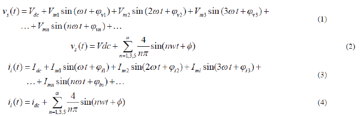 |
| In (1) and (2), subscript‘s’ and ‘l’ stand for supply and load respectively. Subscripts ‘mn’ stands for peak value of nth harmonic and ni φni in general stands for phase angle of nth harmonic component in current. It can be proved that average real power drawn by non-linear load depends upon the voltage and the fundamental component of the load current. The harmonic components of the load current do not contribute to the real power. The instantaneous power is given by, |
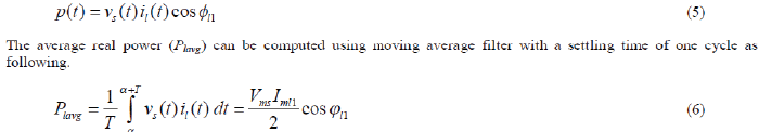 |
| In (5), 1 t is any arbitrary instant and T is the time period of the voltage and current waveform. For 50 Hz ac system, the time period T is 20 ms. If the load current contains only odd harmonic, the averaging time of (5) will be T/2, which is 10 ms. Once we know the average real power of the load, we shall find the reference source current from the source. Let a power factor of cos φs be desired from the source, then following equation is satisfied. |
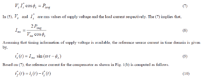 |
| For unity factor operation, cos φs is substituted as 1 in (6). |
| Case 1: To remove only harmonic components of load current |
| In some applications, it is desired that only harmonics components in load current should be eliminated and only fundamental component should come from supply (utility) without any shift in phase angle. To make this type of compensation, it is necessary to know the magnitude and phase angle of the fundamental component of the load current. This is achieved with the help of Fourier transform and its averaging over a complete cycle as illustrated below. |
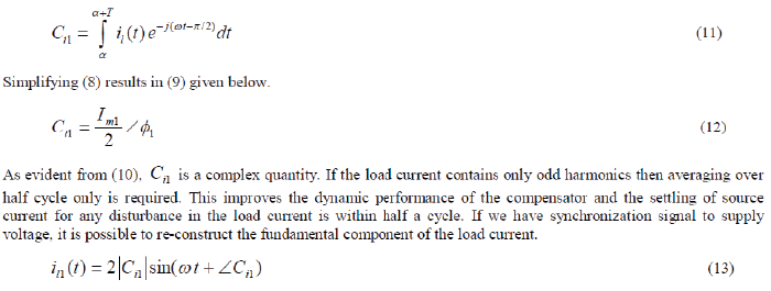 |
| where, |.| and <. are the magnitude and the angle of complex quantity Ci1 respectively. This fundamental component of the load current is to be supplied from the source. The rest of the harmonic components of load current are to be injected from the compensator. Therefore we have, |
 |
| Both of above schemes require the synchronization with the supply voltage and don’t depend on the shape of the supply voltage. Thus the two methods can also be extended to distorted supply voltage provided synchronization information is correct. However when the voltage is distorted, the phase angle between fundamentals of voltage and current is important. |
SIMULATION RESULTS
|
| In the Section II, we have assumed an ideal compensator operation as shown in Fig. 1(a) In this figure, an ideal compensator is represented by an ideal current source ( i*f ). An actual compensator is comprised of full bridge voltage source inverter and a dc storage capacitor. This is shown in Fig. 1(b). The compensator is connected to load at PCC through interface inductor (Lf). The interface inductor includes the leakage inductance of transformer. The resistance Rf models the losses in the inverter. Each IGBT switch in the inverter has an anti-parallel diode to allow the current in both the direction. |
| The reference source current ( i*f ) is extracted using (1) - (14). The reference compensator current ( i*f ) is computed using (9). To realize reference compensator current, the single-phase, full-bridge voltage source inverter is operated in current control in a pre-defined hysteresis band. Thus, the diagonal switches pairs (S1-S2) and (S3-S4) are operated in complimentary mode in such a way so as to track the reference compensator current. Furthermore the compensator has switching losses, therefore dc capacitor must be charged from supply to maintain its voltage near to the reference value. Thus the source must also supply the losses ( loss P ) in the inverter in addition to the average load power. The term loss P is generated by monitoring the dc capacitor average voltage. The average voltage of dc capacitor is held constant if the average value of dc capacitor current over a cycle is zero. The voltage and current relationship for capacitor is given below. |
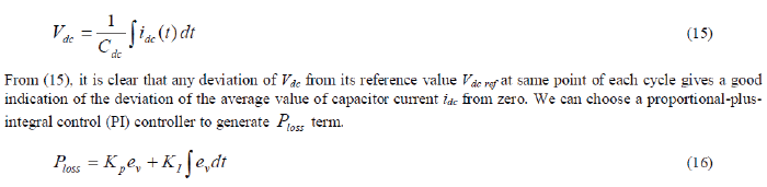 |
| where ev = Vdcp -V dcref ,Vdcp being the value of dc capacitor voltage at same point p of each cycle. This point p in a cycle can be every positive zero crossing of the voltage waveform. The term loss P is incorporated in extraction of compensator reference current by changing lavg P by lavg loss P lavg + Ploss in all above equations, wherever term lavg P is encountered. |
| From the above waveforms the power factor angle is explicitly set to desire one. Initially considered as power as zero angle, waveforms are showing in Fig 2 to 7. From Fig.3 it’s showing that before compensation load current and source current both are same, disturbed because of finite source impedance. In fig4-5 showing that reference and actual filter currents. The reference filter currents are generated using the theory proposed by authors successfully and the power factor is set to desired value. In fig 7 the source voltage and current are in balance, source current is following with source voltage with desired power factor. In fig 7 source current has some notches this is because of bridge rectifier non linear load. From fig 7-11 power factor angle has set to 45 degrees, the wave forms are generated considering with similar properties. The variation of waveforms in reference and actual filter currents are clearly observed with desired power factor, the waveforms are shifted 45 degrees in actual and reference filter currents. In fig 11 also showing that power factor angle, in the same waveforms source voltage and current are balanced. Source current has some notches due rectifier non linear load. |
CONCLUSION
|
| The control algorithm for a single phase shunt active power filter is presented. The method proposed works effectively for both harmonics and load balancing under stiff source and distorted source voltages, currents. The source currents are distorted due to finite impedance of source and distribution transformers. After compensation the source voltage and current are in phase with desired power factor. |
| |
Tables at a glance
|
 |
| Table 1 |
|
| |
Figures at a glance
|
 |
 |
 |
 |
 |
| Figure 1 |
Figure 2 |
Figure 3 |
Figure 4 |
Figure 5 |
| |
 |
 |
 |
 |
 |
| Figure 6 |
Figure 7 |
Figure 8 |
Figure 9 |
Figure 10 |
| |
 |
| Figure 11 |
|
| |
References
|
- J. S. Tepper, J.W.Dixon, G.Venegas and L. Moran, "A simple frequency independent method for calculating the reactive and harmonic currentin a nonlinear load," IEEE Trans. Ind. Electron., vol.43, pp. 647-654, Dec 1996J. Breckling, Ed., The Analysis of Directional Time Series: Applications to Wind Speed and Direction, ser. Lecture Notes in Statistics. Berlin, Germany: Springer, 1989, vol. 61.
- L. Zhou and Z. Li, "A novel active power filter based on the least compensation current control method," IEEE Trans. Power Electron. Vol.15, pp. 655-659, July 2000.M. Wegmuller, J. P. von der Weid, P. Oberson, and N. Gisin, “High resolution fiber distributed measurements withcoherent OFDR,” in Proc. ECOC’00, 2000, paper 11.3.4, p. 109.
- M. K. Ghartemani, H. Mokhtari and M. R. Iravani, "A signal processing system for extraction of harmonics and reactive current of singlephase systems," IEEE Trans. Power Delivery, vol. 19, pp. 979-986, July 2004. (2002) The IEEE website.[Online]. Available: http://www.ieee.org/
- M. T. Haque, "Single phase PQ theory", in PESC 2002, pp. 1815-1820.FLEXChip Signal Processor (MC68175/D), Motorola, 1996.
- M. T. Haque, "Single phase PQ theory for active filters," in proc IEEE TENCON '02, pp. 1941-1944.
- J. C. Wu and H.J. Jou, "Simplified control method for single-phase active power filter," IEE proc. Electric Power Application, Vol. 143, No. 3,pp. 219-224, May. 1996.J. Padhye, V. Firoiu, and D. Towsley, “A stochastic model of TCP Reno congestion avoidance and control,” Univ. ofMassachusetts, Amherst, MA, CMPSCI Tech. Rep. 99-02, 1999.
- D. A. Torrey and A. M. A. M. Al-Zamel, "Single phase active power filter for multiple nonlinear loads," IEEE Trans. Power Electron.,vol. 10, pp. 263-272, May 1995.
- Barsali, S. ;Giglioli, R. ; Monachesi, F. ; Poli, D. "Compensation of voltage unbalances in LV networks due to single-phase generators,"Innovative Smart Grid Technologies Europe (ISGT EUROPE), 2013 4th IEEE/PES, pp. 1-5, May 2013.
- Kanjiya, P. ;Khadkikar, V. ; Zeineldin, H.H. "A Noniterative Optimized Algorithm for Shunt Active Power Filter under Distorted andUnbalanced Supply Voltages," Industrial Electronics, IEEE Transactions on, Volume: 60, Issue: 12 pp. 5376- 5390, May 2013.
- Petkovsek, M. ; Leban, A. ; Nemec, M. ; Voncina, D. ; Zajec, P. "Voltage harmonics compensator for high-voltage power supplies," Compatibility and Power Electronics (CPE), 2013 8th International Conference on, Volume: 60, Issue: 12 pp. 167- 170, 2013.
|