QPSK or Quadrature Phase-Shift Keying is a higher order modulation scheme used in digital modulation. A direct injection locked QPSK modulator uses VCO for minimize the area of the conventional modulator. In this project injection locking scheme is used since injection locking has an advantage inphase-noise reduction ofoscillators withavery simplecircuittopology. By using proposed simple modulator many blocks removed so that total area is reduced. The proposed quadraturephase-shiftkeying (QPSK) was fabricated in 90 nm CMOS, occupies less area.
Keywords |
| CMOS,injectionlocking, modulator,quadrature phase-shiftkeying(QPSK),ringvoltage-controlled
oscillator (VCO) |
INTRODUCTION |
| In satellite or telecommunication system, modulation is the process of conveying a message signal over a medium. To
extend the range of the analog signal or digital data, we need to transmit it through a medium other than air. The
process of converting information so that it can be successfully transmitted through a medium is called modulation. We
are working with QPSK modulation which is kind of a digital modulation. Before going into the main focus we shall
have a brief discussion on modulation, different types of modulation and the analysis of it. |
RELATED WORK |
| In [2] authors present a low power QPSK transmitter for band operating in 405-406MHz frequency range with 10
channels, with 100 KHz channel bandwidth. RF carrier is generated using an injection locked ring oscillator. In [3]
authors used A novel technique for wideband injection locking in an LC oscillator is proposed. Phased-lock-loop and
injection- locking elements are combined symbiotically to achieve wide locking range while retaining the simplicity of
the latter. In [4] authors construct a mixed-mode QPSK demodulator for 60-GHz wireless personal area network
application . The prototype chip realized by 60-nm CMOS process can demodulate up to 4.8-Gb/s QPSK signals at 4.8-
GHz carrier frequency. In [5] present A low-phase-noise integer-N phase-locked loop (PLL) is attractive in many
applications, such as clock generation and analog-to-digital conversion. The sub-harmonically injection-locked
technique, sub-sampling technique, and the multiplying delay-locked loop (MDLL) can significantly improve the phase
noise of an integer-N PLL. |
DIRECT INJECTION-LOCKED QPSK MODULATOR |
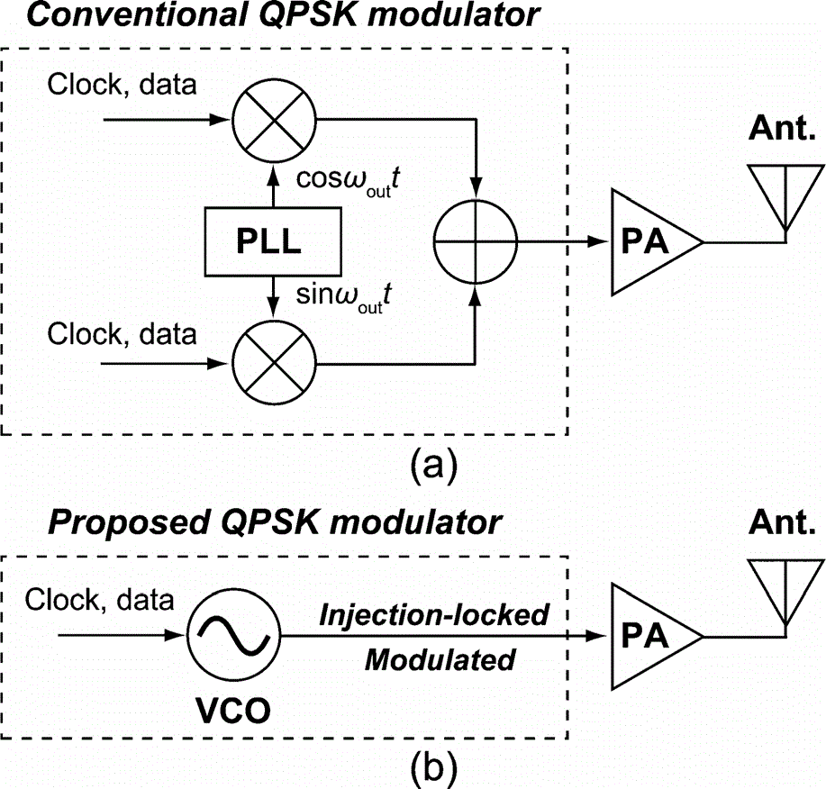
| Fig.1(a) shows conventional QPSK modulator based on a quadrature-output PLL, which employs many RF blocks
such mixers, digital-to-analog converters(DACs),and filters for quadrature mixing[6]. As a consequence, this
structure consumes large area and power to generate quadrature outputs and quadrature mixing. |
| In [7-8], injection locking was employed to generate phase- locked clocks based on ring VCOs. The phase modulation
was achieved in other blocks such as a power amplifier (PA) and a phase multiplexer (MUX) using the phase-locked
clocks. Also, in [3], the phase modulation was directly achieved by adjusting the self-resonant frequency of a n LC
VCO addition to phase locking with injection locking and by using a polarity swap circuit. |
| Proposed QPSK modulator is shown in Fig.1 (b), which uses characteristics of injection locking such as phase
locking and mixing. Phase locking and modulation area achieved by using pulses from the clock and by using the
data which is synchronized with the clock, respectively. Compared within [3], the simple and small one can be
achieved since the proposed QPSK modulator only uses a ring VCO and phase-modulated pulse injection. |
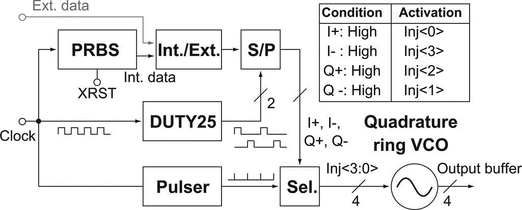
| Fig.2 depicts a detailed block diagram of the proposed QPSK Modulator. It consists of aduty-25% pulse
generator(DUTY25) from the clock, a serial to parallel circuit (S/P),an internal/external data selector, and an internal
pseudo-random bit sequence (PRBS) generator with a sequence length of 27 -1. |
| In this letter, the internal data generated by the PRBS generator was used in the measurement when XRST is high. The
blocks mentioned above have a role to demultiplex the serial input data into the parallel sequences. It also contains a
ring VCO, a pulser, and a pulse selector. The pulse selector selects injection pulses according to the parallel data
sequences (I+, I-, Q+.Q-) as shown in the table of Fig.2.As a result, phase-modulated pulses are injected into the
VCO. |
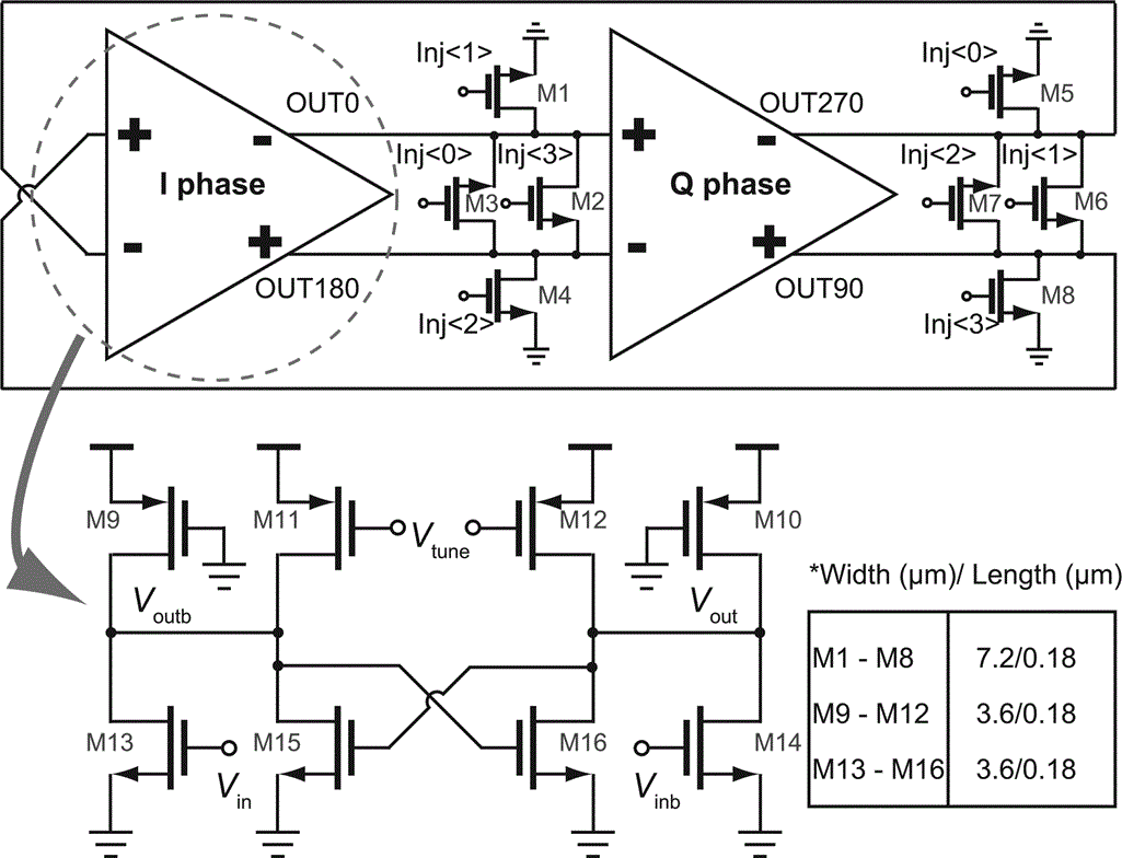
| Fig.4 shows the proposed two-stage quadrature ring VCO. The injection signal is input into both I- phase and Q-phase
delay cell in the form of rail-to-rail pulses for subharmonic i n j e c t i on locking, which are generated by the internal
NAND-based pulser. The pulser can control the pulse width by tuning the control voltage, and generate pulses shorter
than100ps. In this pro- posed ring VCO, NMOS switches(M1, M4,M5,M8) between the output node and the ground as
well as NMOS switches(M2, M3,M6, M7) between the differential outputs are applied. It is to provide the phase shift
with injection pulses to I-and Q-phase outputs simultaneously. The delay cell of this ring VCO contains an NMOS
latch that generates a delay by positive feedback in order to satisfy the oscillation condition. In other words, the latch
has a role of keeping the oscillation even with I/Q pulse injection. The PMOS resistive loads are used for tuning the
output oscillation frequency. The delay cell only contains eight MOSs for simplicity. |
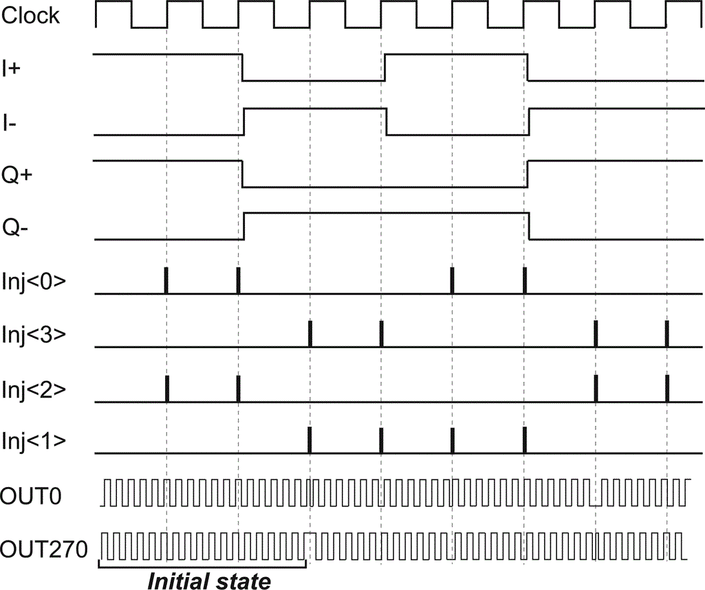
| Fig. 5. shows the mechanism of the proposed QPSK modulator. It shows waveforms of the input clock ,and the parallel
data sequences I+, I- , Q+ ,Q- , the injection pulses ( INJ (3:0) ), and the VCO outputs when it is supposed that the
VCO output frequency (f out) is integer-multiples of clock frequency ( f ref ).Firstly,supposedthattheinitialstateis
thestatelockingtotheinjectionpulsesof INJ (0) and INJ (2). It is determined by the timing of injections and phase
imbalance among the outputs in real world oscillator systems only when sufficiently short pulses are injected. |
CIRCUIT DESIGN |
A.VOLTAGE CONTROLLED OSCILLATORS |
| Voltage controlled oscillators (VCOs) are the Electronic circuits which are used for high speed clock generation,
channel selection, frequency modulation and demodulation in various communication circuits. In the modern
communication system, there is a calculated gap between the adjacent channels for the efficient use of frequency
spectrum. Therefore, in order to avoid interference and noise problem, the characteristics of an oscillator are of much
importance. Among the compilation of signals, oscillator must be able to detect the desired signal. Hence VCO is a
critical component of frequency synthesizer circuits and PLLs. |
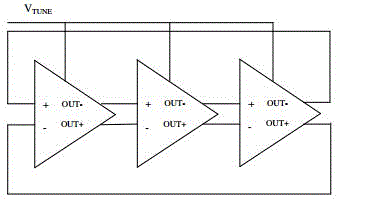
| Like any oscillators, a VCO may be considered as an amplifier and a feedback loop. For the circuit to oscillate the total
phase shift around the loop must be 360 degrees and the gain must be unity. In case of ring oscillators, the delay stages
or cells are connected back to back. If there are N delay stages, the frequency of oscillation is given by f=1/2Ntd where
td is the delay of one delay cell. The less number of delay cells with less propagation delay can increase the frequency
of oscillation. |
B. PHASE LOCKED LOOP |
| Phase-locked loops are widely employed in radio, telecommunications, computers and other electronic applications.
They can be used to demodulate a signal, recover a signal from a noisy communication channel, generate a stable
frequency at multiples of an input frequency (frequency synthesis), or distribute precisely timed clock pulses in digital
logic circuits such as microprocessors. Since a single integrated circuit can provide a complete phase-locked-loop
building block, the technique is widely used in modernelectronic devices, with output frequencies from a fraction of a
hertz up to
many gigahertz. |
| A phase-locked loop or phase lock loop (PLL) is a control system that generates an output signal whose phase is related
to the phase of an input signal. While there are several differing types, it is easy to initially visualize as an electronic
circuit consisting of a variable frequency oscillator and a phase detector. The oscillator generates a periodic signal. The
phase detector compares the phase of that signal with the phase of the input periodic signal and adjusts the oscillator to
keep the phases matched. Bringing the output signal back toward the input signal for comparison is called a feedback
loop since the output is 'fed back' toward the input forming a loop. |
| Keeping the input and output phase in lock step also implies keeping the input and output frequencies the same.
Consequently addition to synchronizing signals, a phase-locked loop can track an input frequency, or it can generate a
frequency that is a multiple of the input frequency. These properties are used for computer clock synchronization,
demodulation, and frequency synthesis. |
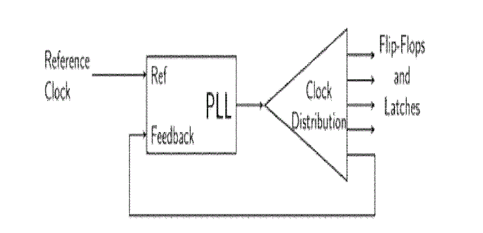
| Typically, the reference clock enters the chip and drives a phase locked loop (PLL), which then drives the system's
clock distribution. The clock distribution is usually balanced so that the clock arrives at every endpoint simultaneously.
One of those endpoints is the PLL's feedback input. The function of the PLL is to compare the distributed clock to the
incoming reference clock, and vary the phase and frequency of its output until the reference and feedback clocks are
phase and frequency matched. |
| PLLs are ubiquitous—they tune clocks in systems several feet across, as well as clocks in small portions of individual
chips. Sometimes the reference clock may not actually be a pure clock at all, but rather a data stream with enough
transitions that the PLL is able to recover a regular clock from that stream. Sometimes the reference clock is the same
frequency as the clock driven through the clock distribution, other times the distributed clock may be some rational
multiple of the reference. |
SIMULATION RESULTS |
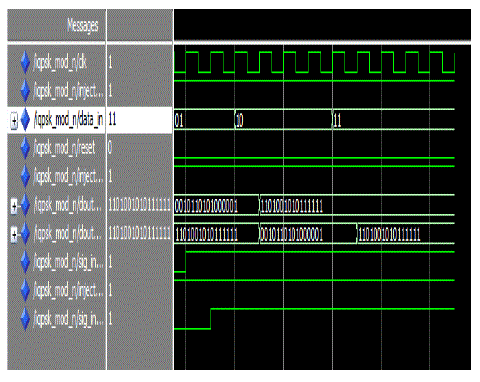
| Fig.8 depicts a simulation waveform of the QPSK modulator with the signals of Injection, reset and data. Rest of the
Fig.9 gives the waveform with injection high with various data. Fig. 10Injection value given as 0 so there is no injected
voltage to VCO, No data available in result. |
CONCLUSION |
| Direct Injection locked QPSK modulator is proposed by replacing many blocks in conventional modulator such that
mixers, analog-to-digital converters and filters so that area of the proposed modulator is reduced. By eliminating
inductor and other PLL blocks, a simple and scalable QPSK modulator is achieved. |
| |
Figures at a glance |
 |
 |
 |
 |
| Figure 1 |
Figure 2 |
Figure 3 |
Figure 4 |
 |
 |
 |
| Figure 5 |
Figure 6 |
Figure 7 |
|
| |
References |
- S. Ye, L. Jansson, and I. Galton, âÃâ¬ÃÅA multiple-crystal interface PLL withVCO realignment to reduce phase noise,âÃâ¬Ã IEEE J. Solid-State
Circuits,vol. 37, no. 12, pp. 1795âÃâ¬Ãâ1803, Dec. 2002.
- J. Lee and H. Wang, âÃâ¬ÃÅStudy of subharmonically injection-lockedPLLs,âÃâ¬Ã IEEE J. Solid-State Circuits, vol. 44, no. 5, pp. 1539âÃâ¬Ãâ1553,May 2009.
- S. Diao, Y. Zheng, Y. Gao, S. Cheng, X. Yuan, M. Je, and C. Heng,âÃâ¬ÃÅA 50-Mb/s CMOS QPSK/O-QPSK transmitter employing injectionlocking for direct modulation,âÃâ¬Ã IEEE Trans. Microw. Theory Tech., vol.60, no. 1, pp. 120âÃâ¬Ãâ130, Jan. 2012.
- J. Bae, K. Song, H. Lee, H. Cho, and H.-J. Yoo, âÃâ¬ÃÅA low-energy crystal-Less double-FSK sensor node transceiver for wireless body-area network,âÃâ¬ÃÂIEEE J. Solid-State Circuits, vol. 46, no. 2, pp. 416âÃâ¬Ãâ423, Feb.2011.
- Q. Zhu and Y. Xu, âÃâ¬ÃÅA 228 m 750 MHz BPSK demodulator basedon injection locking,âÃâ¬Ã IEEE J. Solid-State Circuits, vol. 46, no. 2, pp.416âÃâ¬Ãâ423, Feb. 2011.
- B. Razavi, RF Microelectronics. Upper Saddle River, NJ, USA:Prentice-Hall, 1998.
- M. M. Izad and C. Heng, âÃâ¬ÃÅA 17 pJ/bit 915 MHz 8PSK/O-QPSK transmitterfor high data rate biomedical applications,âÃâ¬Ã in IEEE CICC Dig.,Sep. 2012, pp. 1âÃâ¬Ãâ4.
- H.-C. Chen and W.-K.Lee, âÃâ¬ÃÅBattery-less ASK/O-QPSK transmitterfor medical implants,âÃâ¬Ã Electron.Lett., vol. 48, no. 17, pp. 1036âÃâ¬Ãâ1038,
|