Keywords
|
| Switched-mode power-supply (SMPS), Two Switch Forward Topology, Multiple output converter. |
INTRODUCTION
|
| Many of today's high speed digital logic circuits has many components whichdemands power supply of different voltage levels.The requirement for multiple voltage levels, to support different digital systems, may bedriven by a single dc source, viz., battery. One approach to regulate multiple outputs froma source is to have a single power converter with multiple outputs, e.g., a fly back or forward converter with multiple secondary windings, and regulate the outputs. This approach is more common due to its simplicity; however, a transformer is needed even if isolation is not required. The forward converter is one of the most popular switching topologies for lowand medium power applications. |
| Multiple output converters regulate their main output, from which the feedback signalis generated, with very good accuracy[1]. The other outputs are regulated with lesseraccuracy since they are not part of a closed loop regulation scheme. In applications wheretight voltage regulation of each output is necessary, some sort of post regulation technique isused to regulate the auxiliary outputs of a multiple output converter. Post regulation of theother outputs can be achieved by linear post-regulators, individual DC-DC convertersetc. Linear post-regulators are extensively used for low current outputs. |
| A power distribution system for supplying multiple loads with individually regulatedvoltages from a controlled current source is presented in [2]. Push-pull converter and forward converter are two kinds of popular DC-DC converter[4]. But they have their inherent problems. Transformer in push-pull converter may meetunbalance magnetization and this will result in transformer saturation. Forward converter is very popular in DC-DC application. In low voltage, high currentpower conversion, this topology is also favourable. Primarily, this is because it is the simplestisolated step-down topology [6]. |
| A circuit is proposed to alleviate the problems associated with using synchronous rectifiers in forward converters in [2]. The main feature of the converter is the introductionof an LC snubber circuit on the primary side of the forward converter. But this approach leads to the addition of activeswitch which requires additional gate drive circuit and makes control complicated. The forward converter with the active-clamp reset offers many advantages over the forward converters with other transformer-reset methods [3]. |
| To obtain an isolated power supply, two-switch Forward converters consist in one of themost suitable topologies since the power switches need to block only the supply voltageinstead of twice or more times the supply voltage as in fly back or single-ended Forward converter [7]. |
| The objective of this work is to designand develop a multiple output dc-dc converterbased on Two SwitchForward Converter topology. The DC-DC converter is designed toprovide multiple output power rails for common requirements in industrial applications with input battery supply varies from 24V-36V. Converter works in closed loop mode with necessary compensation circuits to meet the output regulation requirements for change in load. Loop Feedback is closed by make use of control winding. Input output isolation is met using gate drive transformers. The multiple output dc-dc converter is designed and investigated by using ICAP/4 using PWM controller UC1825. The simulation results have demonstrated that the proposed converter delivers constant voltage outputs with high efficiency and reliability. |
| In this paper, a multiple output dc-dc converter. Section II deals with two switch forward converter topology and its operation. In Section III, the circuit analysis of the converter is discussed. Section IV deals with the proposed converter circuit to provide multiple output voltages and component selection. Simulation results to verify the converters’ characteristics are presented in Section V. Finally, Section VI draws the concluding remarks. |
TWO SWITCH FORWARD TOPOLOGY
|
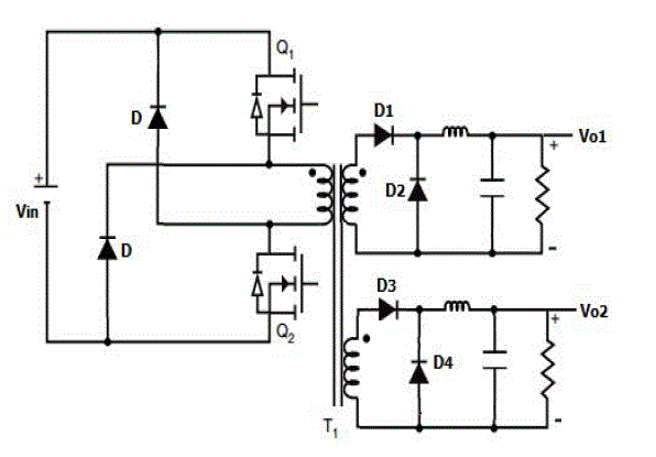
| As the name indicates two switch forward converter topology has two transistorswitches rather than one compared with the single ended forward converter [1]. Figure.1 show a multiple output dc-dc converterbased on Two Switch Forward Converter topology, which delivers multiple power rails. Two switches Q1 and Q2 are in series with the transformer primary. These transistors are turned on and off simultaneously. In the off state, both transistors are subjected to only the DC input voltage rather than twice that, as in the single ended converter. The two switched forward converter works in two modes as follows. |
| A. Mode 1 of Circuit Operation |
| In Mode 1 of circuit of circuit operation, both switches Q1 and Q2 are turned ON. This connects the input voltage source, Vin to the primary winding. Both primary and secondary winding starts conducting simultaneously with the turning on of the switches. Figure 2(a) shows switches Q1 and Q2, which turn on together, transferring energy through the transformer primary into the secondary. On the secondary, the forward rectifying diodeD1 conducts, transferring the energy into the output filter and load. |
| B. Mode 2 of Circuit Operation |
| When transistors Q1 and Q2 are turned OFF, the transformer magnetizing current flows through the now forwardbiased diodes on the primary of transformer and then back into the source as shown in Figure 2(b). Since these forward-biased diodes clamp the input voltage, no snubber circuit is required. On the secondary, the freewheeling diodeD2 conducts as shown, transferring the output inductor energy to the load. |
CIRCUIT ANALYSIS
|
| The working of a multiple output two switch forward converter is shown in Figure 2. It operates in two modes depending upon the condition of the switches Q1 and Q2. In mode 1, switches Q1and Q2, which turns on together, transfers’ energy from input supply through the transformer primary into the secondary. On the secondary, the forward rectifying diode conducts, transferring the energy into the load. In mode 2, when switches Q1and Q2 are OFF, the transformer magnetizing current flows through the forward-biased diodes on the transformer primary and then back into the source. On the secondary, the freewheeling diode conducts as shown, transferring the output inductor energy to the load. |
| The equivalent circuits of mode-1 and mode-2 can be used to derive a steady state relation between the input voltage, switch duty ratio (D) and the output voltage. |
| The inductor voltage (VL) during mode-1 can be written as: |
 |
| The output voltage of forward converter is directly proportional to the duty ratio, D. It may be noticed that except for transformer scaling factor, the output voltage relation is same as in a simple buck converter. |
CIRCUIT DESIGN
|
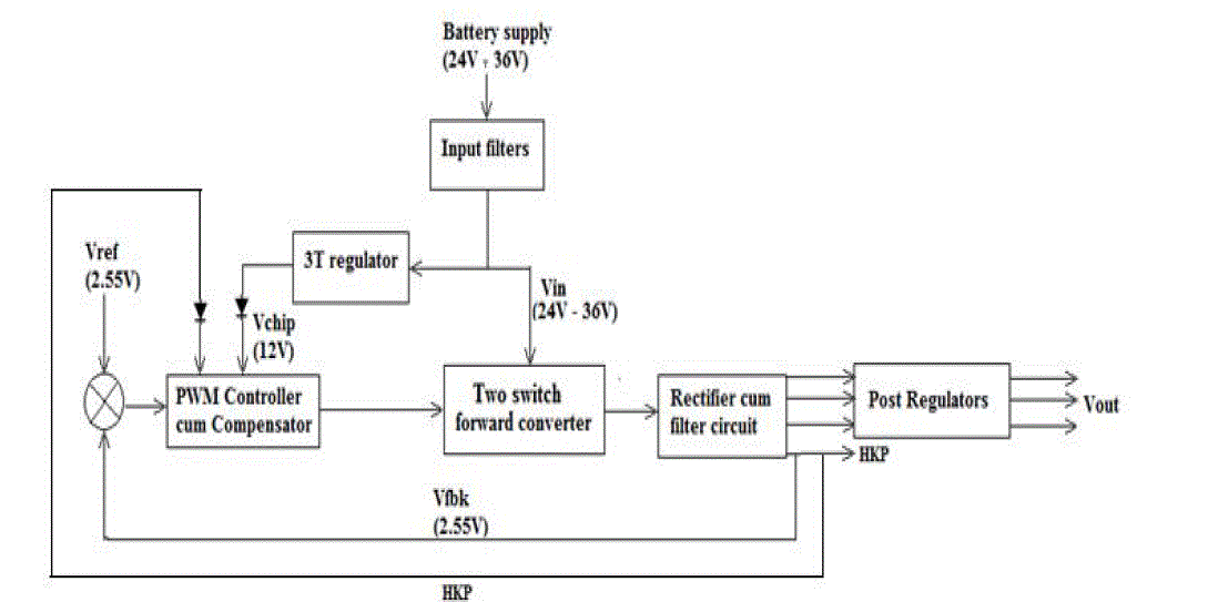
| The block diagram of the proposed DC-DC converter to provide multiple constant output voltagesis shown in figure 3. The input battery supply varies from 24-36 V with a nominal voltageof 28V.The converter is designed to provide multiple voltage outputs (+15V, -15V, 5V) and a house keeping output of 15V.LoopFeedback is closed by making use of house-keeping winding.The requirement specifications of the converter are shown in Table I. |
| The converter consists of two switches which are switched simultaneously by usingPWM controller-UC1825. Input supply for the PWM controller is derived from the inputbattery supply by using 3T regulator, LM117. Converter works in closed loop mode with necessarycompensation circuits to meet the output regulation requirements for change in load. LoopFeedback is closed by making use of house keeping winding. Input output isolation is met usinggate drive transformers. Here the one output i.e. HKP output, from which the feedbacksignal is generated, is regulated with very good accuracy. The auxiliary outputs converteris regulated with lesser accuracy since they are not part of a closed loop regulation scheme.To achieve tight voltage regulation of each output, linear post-regulators are used at each output of the multiple output converter. Once the converter starts working, the input supply for the PWM controller is derived from the house keeping output. |
| A.Switching Transformer |
| The Switching transformer is the heart of the SMPS[8]. It transfers the energy from the source to the converter. Also, it provides isolation between the input power source and the device. The transformer is designed with required turn’s ratio to meet the voltage and current requirements. |
| Turns ratio of switching transformer can be calculated as follows: |
 |
| The size of a power transformer is determined by Area product. An appropriate core will be selected which must have area product greater than the calculated Ap. For a forwardconverter, area product is calculated from the value of output power as: |
 |
| Switching Transformer is designed for maximum allowable flux density Bm= 0.125T, Current density J = 4A/mm2, window utilization factor Kw= 0.4 and efficiency, is takento be 80%. |
| The primary number of turns is selected as N1= 10 turns. |
| The number of turns of secondary-1 = turns ratio1*N1= 18 turns |
| The number of turns of secondary-2 = turns ratio2*N1= 18 turns |
| The number of turns of secondary-3 = turns ratio3*N1= 8 turns |
| The number of turns of secondary-4 = turns ratio4*N1= 16 turns |
| B.Rectifier |
| The diode rectifiers are selected to meet the respective voltage stress and current stress through the diode. Schottky diode, 1N5811 having VRRM of 150V, 3A is selected. |
| C.Output Filter |
| The output filter section of a forward-mode converter (or LC filter) is a series inductor followed by a shunt capacitor. |
| The inductor is used to reduce the ripple current. Output inductance is designed for ripple current of 10%. The output inductance is selected as: |
 |
| Final selection of various components for output filter network based on the equations above are shown in Table III. |
SIMULATION
|
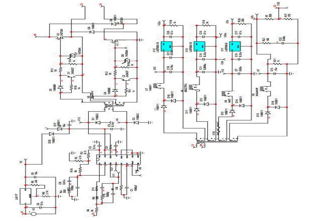
| The simulation of the dc-dc converter was performed using ICAP/4 software. The simulation circuit of the DC-DC converter to provide multiple constant output voltages is shown in figure 4. The simulation is carried out on resistive load with inputbattery supply varies from 24-36 V with a nominal voltage of 28V. The converter is designed to provide multiple voltage outputs (+15V, -15V, 5V) and a house keeping output of 15V. Simulations are carried out for a switching frequency of 250 kHz. |
| The converter consists of two switches which are switched simultaneously by using PWM controller-UC1825. Input supply for the PWM controller is derived from the input battery supply by using 3T regulator, LM117 as shown in Figure 4.Converter parameters in the simulation were discussed in Section III and in Table IV. |
| Simulation waveforms are shown in figure 5, where OUT A and OUT B is the PWMoutputs of UC1825,CLK is the voltage at clock terminal of UC1825, VGDT is voltage atthe secondary of gate drive transformer and, VGS1 and VGS2 are gate driving signals. Thetwo PWM outputs, OUTA and OUB are 1800out of phase as shown in the figure. In the figure, VGS1 andVGS2 show simultaneous switching of the two MOSFET switches. |
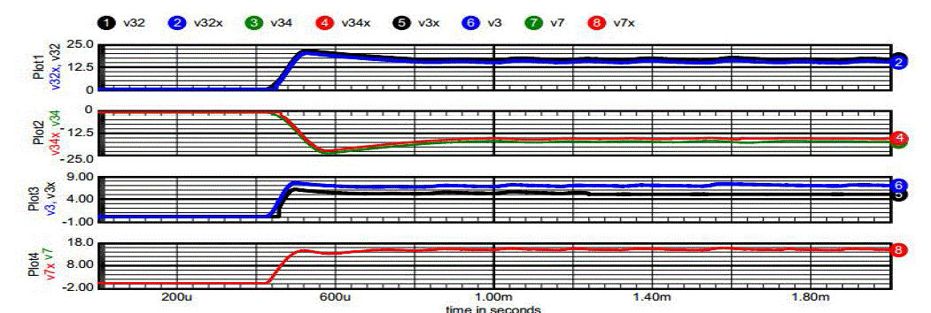
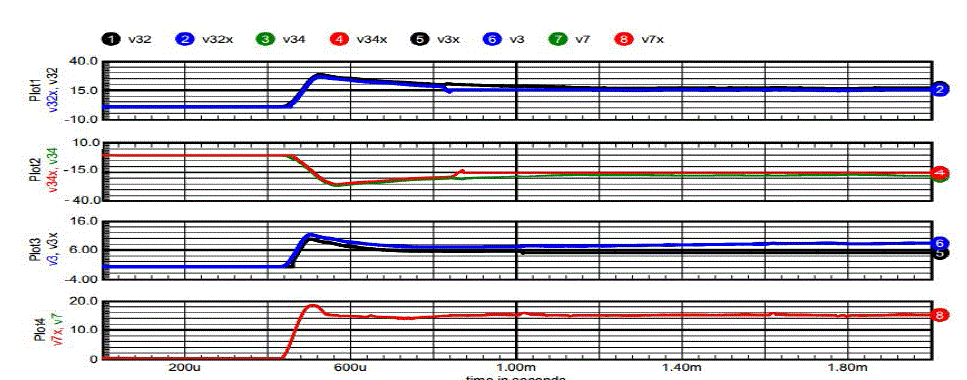
| Unregulated and regulated output waveforms of the proposed converter for minimum and maximum supply voltageare shown in figure 6 and figure 7. Plot 1 shows output voltage at +15V output. Plot 2 shows the output waveforms at -15V output, Plot 3 shows the output waveforms at 5V output, and Plot 4 shows output voltage at the house keeping winding. |
CONCLUSION
|
| In this paper, a multiple output dc-dc converter based on Two Switched Forward topology is proposed. The advantages of this topology include: no need of additional winding in transformer as in single switch topology; thevoltage stress in power switches is limited to maximum supply voltage; snubber circuitry isnot required; the circuit is easy to implement; simplicity of operation over a wide range ofinput voltages and load conditions. |
| In this paper, a multiple output dc-dc converter is designed and developed. The inputbattery supply varies from 24- 36V with a nominal voltage of 28V. The converter delivers constant voltage outputs (+15V, -15V, 5V and+15V HKP) with input output isolation using gate drive transformers. Converter worksin closed loop mode with necessary compensation circuits to meet the output regulationrequirements for change in load. Loop Feedback is closed by make use of control winding.The converter is designed and simulated by using ICAP/4 where PWM controller UC1825 is used to control the switching of the switches. The simulationresults have demonstrated that the proposed converter delivers constant voltage outputs with high reliability. |
Tables at a glance
|
 |
 |
 |
 |
| Table 1 |
Table 2 |
Table 3 |
Table 4 |
|
Figures at a glance
|
 |
 |
 |
 |
| Figure 1 |
Figure 2 |
Figure 3 |
Figure 4 |
 |
 |
 |
| Figure 5 |
Figure 6 |
Figure 7 |
|
References
|
- Abraham I. Pressman, Keith Billings, and Taylor Morey, Switching PowerSupply Design,2nd edition 1998, McGraw-Hill.
- SombuddhaChakraborty, Amit Kumar Jain, Member, and Ned Mohan, “A NovelConverter Topology for Multiple Individually Regulated Outputs," IEEE Trans. PowerElectron., vol. 21, no. 2, pp. 361-369 March 2006.
- PeterMantovanelliBarbosa,and Ivo Barbi, “A Single-Switch Flyback-Current-FedDC-DC Converter," IEEE Trans. Power. Electron., vol. 13, no. 3, pp. 466-475 Mary1998.
- MasahitoJinno, “Effciency Improvement for SR Forward Converters With LC Snubber," IEEE Trans. Power Electron., vol. 21, no. 2, pp. 812- 820 November 2001.
- PradiptaPatra, JyotirmoyGhosh, and AmitPatra, “Control Scheme for Reduced Cross-Regulation in Single-Inductor Multiple-Output DCDCConverters," IEEE Trans. Ind. Electron., vol. 60, no. 11, pp. 5095-5103 November 2013.
- BabakAbdi, JafarMilimonfared and Ahmad MahinFallah , “A High-Performance 1.3KW SMPS with Single Switch Forward Topology," IEEE Trans. Power Electron., vol.24, no. 1, January 2009.
- GiorgioSpiazz, “A High-Quality Rectifier Based on the Forward Topology withSecondary-Side Resonant Reset," IEEE Trans. Ind. Electron., pp. 781-786, 2000. Marty Brown, Practical Switching Power Supply Design, 2002, McGraw- Hill.
- L. Umanand, S.R.Bhatt, Design of magnetic components for Switched Mode PowerConverters.
- Laszlo Balogh, Design And Application Guide For High Speed MOSFET Gate DriveCircuits.
- C.S. Leu, G.C. Hua, F.C. Lee, \Comparison of Forward Topologies With Various ResetSchemes," Virginia Power Electronics Centre.
- Liyu Cao, \Design Type II Compensation In A Systematic Way".
- IRHM7250N HEXFET R Power MOSFET, Note - PD - 90674C, International Rectifier, California.
|