Keywords
|
| Dynamic voltage restorer (DVR), voltage sag, multilevel inverter, THD. |
INTRODUCTION
|
| Voltage sag and voltage swell are two of the most important power-quality (PQ) problems that encompass almost 80% of the distribution system PQ problems [2]. According to the IEEE 1959–1995 standard, voltage sag is the decrease of 0.1 to 0.9 p.u. in the rms voltage level at system frequency and with the duration of half a cycle to 1 min [3]. Short circuits, starting large motors, sudden changes of load, and energization of transformers are the main causes of voltage sags [4]. |
| Among the power quality problems (sags, swells, harmonics…) voltage sags are the most severe disturbances. In order to overcome these problems the concept of custom power devices is introduced recently. One of those devices is the Dynamic Voltage Restorer (DVR), which is the most efficient and effective modern custom power device used in power distribution networks. DVR is a recently proposed series connected solid state device and is normally installed in a distribution system between the supply and the critical load feeder at the point of common coupling (PCC).It employs a series of voltage boost technology using solid (static) state switches of Three Phase VSC that injects voltage into the system; to restore the load side voltage for compensating voltage sags/swells. Other than voltage sags and swells compensation, DVR can also added other features like: line voltage harmonics compensation, reduction of transients in voltage and fault current limitations. |
| In this paper, initially a multifunctional control system is proposed in which the DVR protects the load voltage using charge regulator and P+Resonant controllers when the source of disturbance is the parallel feeders. This is further modified by the introduction of a multilevel inverter system which further improves the performance of the DVR system and provides a better compensation to the voltage sag applied. The THD analysis in each case is also done to estimate the capability of the DVR to limit the harmonics. |
| The remainder of this paper is organized as follows: The general operation of DVR and its state space description are provided in Section II. The closed-loop control using P+Resonant controller and charge regulator has been presented in Section III. In Section IV, the multilevel DVR is introduced. Finally, the simulation results are provided in Section V which shows that the control capability of the proposed DVR system is satisfactory. |
DVR COMPONENTS AND ITS BASIC OPERATIONAL PRINCIPLE
|
| A. DVR Components |
| A typical DVR-connected distribution system is shown in Fig. 1, where the DVR consists of essentially a seriesconnected injection transformer, a voltage-source inverter, an inverter output filter, and an energy storage device that is connected to the dc link. Before injecting the inverter output to the system, it must be filtered so that harmonics due to switching function in the inverter are eliminated. It should be noted that when using the DVR in real situations, the injection transformer will be connected in parallel with a bypass switch (Fig. 1). When there is no disturbances in voltage, the injection transformer (hence, the DVR) will be short circuited by this switch to minimize losses and maximize cost effectiveness. It is obvious that the flexibility of the DVR output depends on the switching accuracy of the pulse width modulation (PWM) scheme and the control method. |
| B. Basic Operational Principle of DVR |
| The DVR system shown in Fig. 1 controls the load voltage by injecting an appropriate voltage phasor in series with the system using the injection series transformer. In most of the sag compensation techniques, it is necessary that during compensation, the DVR injects some active power to the system. Therefore, the capacity of the storage unit can be a limiting factor in compensation, especially during long-term voltage sags. |
| The phasor diagram in Fig. 2 shows the electrical conditions during voltage sag, where, for clarity, only one phase is shown. Voltages V1,V2, Vdvr and are the source-side voltage, the loadside voltage, and the DVR injected voltage, respectively. Also, the operators I, ø , ∂ and α are the load current, the load power factor angle, the source phase voltage angle, and the voltage phase advance angle, respectively. Due to the existence of semiconductor switches in the DVR inverter, this piece of equipment is nonlinear. However, the state equations can be linearized using linearization techniques. The dynamic characteristic of the DVR is influenced by the filter and the load. |
| The P+ Resonant controller works by pole elimination and proper regulation of its parameters is necessary. The feedback path consists of an outer voltage loop and a fast inner current loop. To eliminate the steady-state voltage tracking error (VL* - VL) , a computationally less intensive P+Resonant compensator is added to the outer voltage loop. The ideal P+Resonant compensator can be mathematically expressed as |
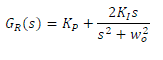 (1) (1) |
| Where Kp and K1 are gain constants and W0 = 2Π *50 rad/sec is the controller resonant frequency. Theoretically, the resonant controller compensates by introducing an infinite gain at the resonant frequency of 50 Hz to force the steady-state voltage error to zero. The ideal resonant controller, however, acts like a network with an infinite quality factor, which is not realizable in practice. A more practical (non ideal) compensator is therefore used here, and is expressed as |
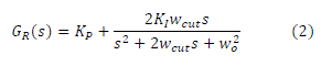 |
| Where Wcutt is the compensator cutoff frequency which is 1 rad/s in this application. |
| Plotting the frequency response of (2), as in Fig. 3, it is noted that the resonant peak now has a finite gain of 40 dB which is satisfactorily high for eliminating the voltage tracking error [13]. In addition, a wider bandwidth is observed around the resonant frequency, which minimizes the sensitivity of the compensator to slight utility frequency variations. |
| In this part, an algorithm is proposed for the DVR to restore the PCC voltage, limit the fault current, and, therefore, protect the DVR components. The flux-charge model here is used in a way so that the DVR acts as a virtual inductance with a variable value in series with the distribution feeder. To do this, the DVR must be controlled in a way to inject a proper voltage having the opposite polarity with respect to usual cases. |
| The proposed DVR control method is illustrated in Fig. 4. It should also be noted that the reference flux (φref is derived by integration of the subtraction of the PCC reference voltage (V*PCC ) and the DVR load-side voltage. In this control strategy, the control variable used for the outer flux model is the inverter-filtered terminal flux defined as: |
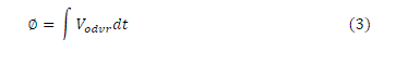 |
| Where Vodvr is the filter capacitor voltage of the DVR (at the DVR power converter side of the injection transformer). The flux error is then fed to the flux regulator, which is a P+Resonant controller, with a transfer function given in (2). On the other hand, it can be shown that a single flux-model would not damp out the resonant peak of the LC filter connected to the output of the inverter. |
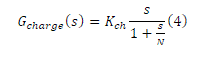
| To stabilize the system, an inner charge model is therefore considered. In this loop, the filter inductor charge, which is derived by integration of its current, tracks the reference charge output Qref of the flux regulator. The calculated charge error is then fed to the charge regulator with the transfer function |
 |
 |
THREE PHASE MULTILEVEL DVR SYSTEM USING PHASE OPPOSITION DISPOSITION STRATEGY
|
| In recent years, industry has begun to demand higher power equipment, which now reaches the megawatt level. Controlled AC drives in the megawatt range are usually connected to the medium-voltage network. Today, it is hard to connect a single power semiconductor switch directly to medium voltage grids. For these reasons, a new family of multilevel inverters has emerged as the solution for working with higher voltage levels. Depending on voltage levels of the output voltage, the inverters can be classified astwo-level inverters and multilevel inverters. The inverters with voltage level 3 or more are referred as multilevel inverters. Multilevel inverters have become attractive recently particularly because of the increased power ratings, improved harmonic performance and reduced EMI emission that can be achieved with the multiple DC levels that are available for synthesis of the output voltage. Xiaoming Yuan and Ivo Barbi [23] proposed fundamentals of a new diode clamping multilevel inverter. |
| The general structure of the multilevel inverter is to synthesize a sinusoidal voltage from several levels of voltages typically obtained from capacitor voltage sources. Multilevel inverters are being considered for an increasing number of applications due to their high power capability associated with lower output harmonics and lower commutation losses. Multilevel inverters have become an effective and practical solution for increasing power and reducing harmonics of AC load. The main multilevel topologies are classified into three categories: diode clamped inverters, flying capacitor inverters, and cascaded inverters. |
| A. PODPWM Strategy |
| In the Phase Opposition Disposition Strategy the carrier waveforms are arranged so that all carrier waveforms above zero are in phase and they are 180 degrees out of phase with those below zero. |
SIMULATION RESULTS
|
| Simulation in general terms can be defined as the representation of a system in its realistic form. When a computer program is used to create a model to mimic a real world system, then the term ‘computer simulation’ comes into action such models are called computer simulated models. |
| Here a test system is designed with the source having a voltage of 22kV supplying a critical load which is a three phase series RLC load with an active power of 100W and the distribution side operates at a voltage of 415V.The controls shown in fig. 4 was applied along with a six pulse inverter circuit. The DC supply (battery storage) was chosen as 210V. Proper filter circuits are also incorporated to eliminate the switching harmonics in the inverter circuit. |
| To observe the functioning of the DVR system a sudden load of 10MW was applied to the system within the time period from t = 0.3 sec to t = 0.6 seconds by using the breaker operation. This causes a voltage sag in the system which also affects the critical load. At this instant the DVR starts compensating for the voltage drop and restores both the critical load voltage as well as the source voltage. This is shown in Fig.5. |
| The THD analysis of the above mentioned system is also done and from the analysis, it can be seen that the distortions in the load voltage is reduced to a considerable extent by the use of the P + Resonant controller in the system. This is represented in Fig. 6. |
| To improve the performance of the DVR used in the voltage compensation, the six pulse inverter circuit is replaced by a three phase fifteen level inverter circuit. This ensures a better voltage at the critical load as well as at the grid side during the event of voltage sag. The technique here applied is the phase opposition disposition PWM strategy and is found very useful in handling systemswith more power. The voltage sag is applied from t = 0.1 sec to t = 0.3 seconds. The simulation results are shown in fig. 7. |
| The THD analysis of the above system is also found out and from the analysis it can be evaluated that the THD value is comparatively low in comparisonto the large number of switching devices used. This is indicated in fig. 8. |
CONCLUSION
|
| In this paper, a multifunctional DVR is proposed, and a closed-loop control system is used for its control to improve the damping of the DVR response. Also, for further eliminating the steady-state error and improving the stability of the system, the P + Resonant controller and charge regulator are used. As the second function of this DVR, using the flux-charge model, the equipment is controlled so that it limits the downstream fault currents and protects the PCC voltage during these faults by acting as variable impedance. The problem of absorbed active power is solved by entering impedance just at the start of this kind of fault in parallel with the dc-link capacitor and the battery being connected in series with a diode so that the power does not enter it. The simulation results verify the effectiveness and capability of the proposed DVR in compensating for the voltage sags caused by sudden switching of a load and limiting the downstream fault currents and protecting the PCC voltage. This paper can be extended to investigate the 3-phase 4- wire system in the near future. We can incorporate other renewable energy sources in the storage system for future developments. |
 |
Figures at a glance
|
 |
 |
 |
 |
| Figure 1 |
Figure 2 |
Figure 3 |
Figure 4 |
 |
 |
 |
 |
| Figure 5 |
Figure 6 |
Figure 7 |
Figure 8 |
|
References
|
- F. Mohammad Mahdianpoor, Rahmat Allah Hooshmand and Mohammad Ataei, “A New Approach to Multifunctional DynamicVoltage Restorer Implementation for EmergencyControl in Distribution Systems,”IEEE Trans. PowerDel., vol. 26, no. 2, april 2011.
- J. A. Martinez and J. Martin-Arnedo, “Voltage sag studies in distribution networks- part II: Voltage sag assessment,” IEEE Trans. PowerDel.,vol. 21, no. 3, pp. 1679–1688, Jul. 2006.
- J. A. Martinez and J. M. Arnedo, “Voltage sag studies in distribution networks- part I: System modeling,” IEEE Trans. Power Del., vol. 21, no. 3, pp. 338–345, Jul. 2006.
- P. Hcine and M. Khronen, “Voltage sag distribution caused by power system faults,” IEEE Trans. Power Syst., vol. 18, no. 4, pp. 1367–1373, Nov. 2003.
- S. S. Choi, B. H. Li, and D. M. Vilathgamuwa, “Dynamic voltage restoration with minimum energy injection,” IEEE Trans. Power Syst., vol. 15, no. 1, pp. 51–57, Feb. 2000.
- C. Fitzer, M. Barnes, and P. Green, “Voltage sag detection technique for a dynamic voltage restore,” IEEE Trans. Ind. Appl., vol. 2, no. 1, pp.203–212, Jan./Feb. 2004.
- C. Benachaiba and B. Ferdi, “Voltage quality improvement using DVR,” Electt.Power Qual. Utilisation, Journal, vol. XIV, no. 1, 2008.
- D. M. Vilathgamuwa, H. M. Wijekoon, and S. S. Choi, “A novel technique to compensate voltage sags in multiline distribution system-the interline dynamic voltage restorer,” IEEE Trans. Ind. Electron., vol. 53, no. 5, pp. 1603–1611, Oct. 2006.
- J. G. Nielsen, M. Newman, H. Nielsen, and F. Blaabjerg, “Control and testing of a dynamic voltage restorer (DVR) at medium voltage level,” IEEE Trans. Power Electron., vol. 19, no. 3, pp. 806–813, May 2004.
- M. J. Newman, D. G. Holmes, J. G. Nielsen, and F. Blaabjerg, “A dynamic voltage restorer (DVR) with selective harmonic compensation at medium voltage level,” IEEE Trans. Ind. Appl., vol. 41, no. 6, pp. 1744–1753, Nov./Dec. 2005.
- A. K. Jindal, A. Ghosh, and A. Joshi, “Critical load bus voltage control using DVR under system frequency variation,” Elect. Power Syst. Res., vol. 78, no. 2, pp. 255–263, Feb. 2008.
- Y. W. Li, D. M. Vilathgamuwa, P. C. Loh, and F. Blaabjerg, “A dualfunctional medium voltage level DVR to limit downstream fault currents,” IEEE Trans. Power Electron., vol. 22, no. 4, pp. 1330–1340, Jul. 2007.
- P. C. Loh, D. M. Vilathgamuwa, S. K. Tang, and H. L. Long, “Multilevel dynamic voltage restorer,” IEEE Power Electron. Lett., vol. 2, no. 4, pp. 125–130, Dec. 2004.
- E. Babaei, M. Farhadi, and M. Sabahi, “Compensation of voltage disturbances in distribution systems using single-phase dynamic voltage restorer,” Elect. Power Syst. Res., Jul. 2010.
- C. N.-M. Ho and H. S.-H. Chung, “Implementation and performance evaluation of a fast dynamic control scheme for capacitor-supported interline DVR,” IEEE Trans
- M. Vilathgamuwa, A. A. D. R. Perera, and S. S. Choi, “Performance improvement of the dynamic voltage restorer with closed-loop load voltage and current-mode control,” IEEE Trans. Power Electron., vol. 17, no. 5, pp. 824–834, Sep. 2002.
- Y. W. Li, P. C. Loh, F. Blaabjerg, and D. M.Vilathgamuwa, “Investigation and improvement of transient response of DVR at medium voltage level,” IEEE Trans. Ind. Appl., vol. 43, no. 5, pp. 1309–1319, Sep./Oct. 2007.
- H. Kim and S. K. Sul, “Compensation voltage control in dynamic voltage restorers by use of feedforward and state feedback scheme,” IEEE Trans. Power Electron., vol. 20, no. 5, pp. 1169–1177, Sep. 2005.
- M. I. Marei, E. F. El-Saadany, and M. M. A. Salama, “A new approach to control DVR based on symmetrical components estimation,” IEEETrans. Power Del., vol. 22, no. 4, pp. 2017–2024, Oct. 2007.
- Y. W. Li, D. M. Vilathgamuwa, F. Blaabjerg, and P. C. Loh, “A robust control scheme for medium-voltage-levelDVR implementation,” IEEETrans. Ind. Electron., vol. 54, no. 4, pp. 2249–2261, Aug. 2007.
- S. A. Saleh, C. R. Moloney, and M. A. Rahman, “Implementation of a dynamic voltage restorer system based on discretewavelet transforms,” IEEE Trans. Power Del., vol. 23, no. 4, pp. 2360–2375, Oct. 2008.
- C. R. Balamurugan, S. P. Natarajan and R. Bensraj,”Investigations on Three Phase Five Level Diode Clamped Multilevel Inverter,” International Journal of Modern Engineering Research (IJMER) www.ijmer.com Vol.2, Issue.3, May-June 2012.
- Xiaoming Yuan and Ivo Barbi “Fundamentals of a New Diode Clamping Multilevel Inverter”, IEEE Trans. on Power Electronics, Vol.15, No.4, 2000, pp.711-718. Power Electron., vol. 25, no. 8, pp. 1975–1988, Aug. 2010.
|