Keywords
|
| Small-signal amplifiers, Darlington pair, JFET Darlington pair, RC coupled amplifiers |
INTRODUCTION
|
| To amplify signals through Darlington pair is an important phenomenon of electronics [1]-[3]. This paired unit of vital importance conventionally holds two identical BJTs in CC-CE connection and its application range is virtually extended from small-signal amplifiers to power amplifier circuits [1]-[3]. Principally, with high input resistance, low output resistance and voltage gain just greater than unity, the current gain factor of Darlington pair (βD) is treated as identical to the product of current gains of the individual transistors (βD≈βQ1.βQ2) [1], [3]. However, as a major drawback, its frequency response exhibits a problem of poor response at higher frequencies [1]-[4]. A number of modifications in Darlington’s composite unit or in respective amplifier circuits are suggested by researchers to overcome this problem [2], [4]-[6]. These efforts include the use of devices other than BJTs or hybrid combination of active devices (e.g. BJT-JFET or BJT-MOSFET etc.) in Darlington’s topology and, moreover, using some additional biasing components in associated amplifier circuit [7]-[10]. Experimentation with Darlington pair topology is still a popular topic for electronic circuit designers to work with [2],[6],[11]-[12]. |
| Present investigation is focused around a Darlington pair which uses two identical JFETs in its composite unit. This pair with appropriate biasing component is explored as new circuit model of a small-signal amplifier suitable for radio and TV receiver stages. |
CIRCUIT DETAILS
|
| Present work comprises a qualitative comparison between small-signal conventional Darlington pair amplifier (Fig.1) and a new circuit of small-signal amplifier which is having identical JFETs in Darlington pair configuration (Fig.2) and an additional biasing resistance in the circuit. |
| Conventional Darlington pair amplifier [1]-[2],[4],[6],[11] of Fig.1 is named as Reference Amplifier for the present studies whereas the Proposed Amplifier circuit of Fig.2 is obtained by replacing paired BJTs of the circuit of Fig.1 with that of identical JFETs. In addition, the proposed amplifier circuit also uses an additional biasing resistance RA [2],[4],[6] between source of J1 and ground. Amplifier circuits under discussion use potential divider biasing methodology [4],[6]- [7] with properly selected passive biasing components. Component details of respective circuits are summarized in TABLE I. |
| PSpice simulation (Student version 9.2) is performed to carry out present investigations [15]. Observations are procured by feeding the amplifier circuits with 1V AC input signal source, from which, a small-distortion-less AC signal of 1mV for reference amplifier (Fig.1) and 30mV for proposed amplifier (Fig.2) at 1KHz frequency is drawn as input for the amplification purpose. |
| Amplifiers of Fig.1 and Fig.2 provide fair and distortion-less results in 1-10mV and 1-80mV range of AC input signals respectively at 1KHz frequency. However the best results for reference and proposed amplifiers are received at 1mV and 30mV AC inputs respectively. |
OBSERVATIONS AND DISCUSSIONS
|
| A. Qualitative Performance |
| Fig.3 depicts the variation of voltage gain as a function of frequency. At biasing parameter values of TABLE I, the reference amplifier produces 16.98 maximum voltage gain AVG (with 17.328mV peak output voltage), 8.51 maximum current gain AIG (with 1.7327μA peak output current) and 102.058KHz bandwidth BW (with fL=79.913Hz and fH=102.138KHz) [1]-[2],[4],[6],[11] whereas the proposed amplifier generates 9.1084 maximum voltage gain AVG (with 269.696mV peak output voltage), 530.909 maximum current gain AIG (with 26.971μA peak output current) and 12.365MHz bandwidth BW (with fL=88.207Hz and fH=12.366MHz). In addition, if values of coupling capacitors C1 and C2 are reduced to 0.1uF, the bandwidth of the proposed amplifier enhances nominally to reach at 12.548MHz whereas AIG reduces to 526.883 with almost no change in AVG. Though the observed value of AVG of the proposed amplifier is less than reference amplifier but this amount is still significant for small-signal JFET amplifiers. In addition, the proposed amplifier also crops considerably wide bandwidth and high current gain and successfully removes the poorresponse- problem of conventional Darlington pair amplifier (Fig.1) at higher frequencies. |
| Both the amplifiers of Fig.1 and Fig.2 invert phase of voltage or current in amplification mode [1]-[2],[13]. In fact, BJTs in paired unit of reference amplifier hold CC-CE configuration and a CC configuration independently do not show any phase shift between applied input and amplified output signals whereas CE configuration produces an amplified output having 180o phase difference with input. Therefore the resultant paired unit of CC-CE BJTs reverts the phase of output waveform. The similar situation appears for proposed amplifier which holds a CD-CS configuration of JFETs with a property that CD configuration does not reverses the phase whereas CS configuration inverts the phase of output waveform in amplification process. |
| Variation of AVG, AIG and bandwidth with temperature for both the amplifiers is also measured and listed in TABLE II. Bandwidth of the reference amplifier remains unchanged whereas both varieties of gains increase with rising temperature. However, bandwidth of the proposed amplifier mildly increases but voltage and current gains significantly decrease at rising temperature. This decrement in AIG and AVG is associated with ‘negative temperature coefficient’ property of drain current [13]. The drain current in JFET is mainly composed of majority carriers whose mobility decreases at elevated temperature due to enhanced collision rate between them and the remaining ions in the semiconductor channel [13]. This decreases the drain current and therefore the effective current and voltage gain of the JFET based Darlington pair system. |
| Performance of the proposed amplifier highly depends on the presence of additional biasing resistance RA. Variation of maximum voltage and current gains with RA is also observed but results are not shown in form of graphs. It is noticed that the proposed amplifier with RA=3KΩ crops AIG=378.427 and AVG=6.4925 which climbs-up to AIG=546.817 and AVG=9.3786 at RA=1MΩ. This happens because on increasing RA, the gate potential of J2 increases and allows N-type channel to bear a flow of more majority carriers which causes an enhancement in drain current and therefore the load current and current gain. If RA is removed from the proposed circuit, the AIG of the amplifier reaches below unity to a value 0.487 whereas AVG to a non-significant value of 0.118. Conclusively, the presence of additional biasing resistance RA in the proposed configuration is essential to establish ‘JFET Darlington pair unit’ suitable for amplification of small-signals. |
| The input and output noises for proposed amplifier at 100Hz, 1KHz and 1MHz frequencies are observed and respective values are listed in TABLE III. Usually, resistors and semiconductor devices in electronic circuits are responsible to generate noises during amplification process. Table clearly indicates that levels of input and output noises are significantly low for proposed amplifier and within the permissible limit. Both varieties of noises reduce with elevation of operating frequency. Moreover, it also increases with temperature which is an obvious feature due to generation of more carriers and their higher collision rate at elevated temperature. |
| Total Harmonic Distortion (THD) percentage is also calculated for 8 significant harmonic terms using established rules [1],[12],[16]. It is found that the reference amplifiers shows 0.72% THD whereas the proposed amplifier shows 2.15% THD. THDs of both the amplifiers can be significantly reduced by increasing load resistance RL, but this simultaneously reduces the voltage and current gains of the respective amplifiers. TABLE IV shows AVG, AIG and THD at increasing values of Load Resistance RL. |
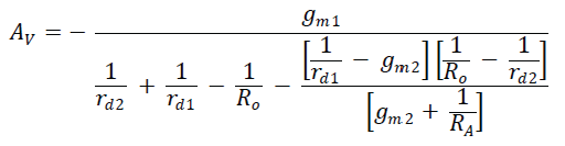
| Small-signal AC equivalent circuit of proposed amplifier is drawn in Fig.4. AC analysis of this amplifier shows that its equivalent output resistance RO≈RL||RD is lower (≈1.66KΩ) than the equivalent input resistance RI≈R1||R2 (≈0.58MΩ), with a phase reversal in output voltage waveform. In addition, AC voltage gain of the proposed amplifier is estimated to be the following and therefore figured out to be -14.076 [1] which is approximately five point higher than the observed value. Here the computed rd1=1.77KΩ, rd2=2.06KΩ, gm1=0.0077mho and gm2=0.0055mho. Negative sign in the expression shows phase reversal of the output voltage which is because the composite unit of JFET Darlington pair holds an equivalent CS configuration [1]. |
 |
| Voltage and current gain of the corresponding amplifiers highly depends on Emitter resistance (for reference amplifier) or source resistance (for proposed amplifier). Respective observations are shown in Fig.5. Voltage gain of the reference amplifier is found to decrease exponentially whereas current gain decreases nonlinearly at increasing values of RE. However, voltage and current gain of the proposed amplifier increases up to 10KΩ, thereafter, decreases exponentially at increasing values of RSR. |
| Performance parameters AVG, AIG and BW at different values of Collector resistance RC (for reference amplifier) and Drain resistance RD (for proposed amplifier) are also estimated but not shown graphically. For reference amplifier, respective parameters behave in the similar way as was observed by Tiwari et.al. [4],[6] and Sayed et.al.[2]. However, for proposed amplifier, voltage gain (2.66) and current gain (155.236) are found at lowest but bandwidth (52.089MHz) at highest for RD=500Ω whereas for RD=2KΩ voltage gain (9.108) and current gain (530.909) are found at maximum but bandwidth (12.365MHz) at minimum. The proposed amplifier yields a poor response at lower frequencies if RD is raised beyond critical value of 2KΩ. Performance parameters are also estimated at different values of DC supply voltage VCC for reference and proposed amplifiers but not shown graphically. Observations indicate that the voltage gain (9.10), current gain (10.12) and bandwidth (12.365MHz) for proposed amplifier are found at lowest for VCC=15V whereas for VCC=30V voltage gain (11.91), current gain (694. 07) and bandwidth (14.923MHz) attain their maximum. The proposed amplifier yields a poor response if VCC is raised above 30V or lowered below 15V. Variation of maximum voltage gain with load resistance RL is also observed but not shown in form of graphs. Observations shows that gain value rises up continuously in low resistance range up to 50KΩ value of RL whereas at higher RL values it approaches towards a sustained level. This nature is well in accordance of the basic nature of small-signal amplifiers [2],[6],[16]. |
| B. Tuning Performance |
| Tunned amplifiers are frequently used in designing Radio or TV receiver type systems [11],[13]. The common practice used to design such amplifiers is to introduce a parallel tuning network (usually L-C-R) at their output or input section. If central frequency of the response is so adjusted to match with the frequency of a particular channel, desired signal can be received. Motayed et.al.[11] had already floated the idea behind tuning of a small-signal CC-CE Darlington pair amplifier (Fig.1), therefore, objective of the present investigation is also to extend the design of proposed amplifier to behave as a successful tuned-amplifier. |
| The tunning performance of the proposed amplifier is established in two steps- first, with RSR-CSR network available at the source end of J2 (Fig.2) and second by introducing a tunning capacitor CL across the load RL (indicated as doted lines in Fig.2). Respective observations are listed in TABLE V. |
| Tunning performance of the proposed amplifier with source bypass capacitor CSR is obtained for variations between 0.01μF and 10μF. Changes in the CSR merely create any variation in voltage gain, whereas it significantly changes current gain and plays a prime role in adjusting the mid-bandwidth (e.g. for CSR=0.01μF, bandwidth extends between fL=87.471KHz and fH=12.485MHz). Other values of Upper and Lower Cut-off frequencies for different CSR can be observed in TABLE V. It is evident from TABLE V that fH varies in a non-significant range with CSR whereas fL considerably shifts towards lower values at increasing CSR. |
| Similarly the inclusion of capacitor CL across load resistance RL also plays an important role in adjusting mid-band frequency range for proposed amplifier. Tunning is obtained for variations of CL between 100pF and 100nF with a feature that the bandwidth of the amplifier shifts towards lower range (from MHz to KHz range) on the frequency axis. Voltage gain, current gain and lower-cut-off frequency varies in a very short range for corresponding variations in CL, whereas, the upper-cut-off limit of the bandwidth shifts towards lower values with increasing CL. |
| Conclusively, adjustment of CSR and CL will lead to a tunning which finally ascertain the frequency response of the proposed amplifier to peak around the desired frequency. This may enable the central frequency of the response to coincide with the frequency of a desired communication channel. This tunning idea is depicted in Fig.6 for two different combinations of CSR and CL. The explored idea of tuning in Fig.6 leads to a conclusion that CD-CS combination in JFET Darlington pair configuration can be applied to receive signal of a specific channel by filtering-out or attenuating others. |
CONCLUSION
|
| As a novel approach, two identical JFETs are used in Darlington pair to explore the proposed circuit as small-signal wide-band amplifier. The proposed amplifier can be tuned in permissible audible frequency range approximately extended from 90Hz to 19KHz. The additional biasing resistance RA (ranging in between 3KΩ to 1MΩ), is to be essentially included in the proposed circuit to maintain its voltage/current amplification property. In absence of RA, amplifier’s voltage and current gains climbs-down below unity and makes it purpose-less. This amplifier can effectively process small-signals ranging below 80mV in the frequency band of 88.2074Hz to 12.366MHz at 1KHz input frequency and is free from the problem of poor response of conventional small-signal Darlington pair amplifiers at higher frequencies. With sufficiently wide bandwidth, high current gain, and a voltage gain noticeably greater than unity, the proposed amplifier generates only 2.15% harmonic distortion which is fairly adaptive for small-signal amplifiers. Observed values of voltage and current gains logically set the power gain of the proposed amplifier considerably larger than unity. Collectively, these features provide a unique flavour to the proposed amplifier in the respective class of JFET based small-signal audio amplifiers. The proposed amplifiers shows a considerable response for VCC, RSR, RD and RL almost in the same way as is usually observed for small-signal RC coupled Common Source amplifiers. |
ACKNOWLEDGMENT
|
| Authors gratefully acknowledge the facilities provided by the Department of Physics and Electronics, Dr. Ram Manohar Lohia Avadh University, Faizabad, U.P., India for the present investigations. |
Tables at a glance
|
 |
|
|
|
|
| Table 1 |
Table 2 |
Table 3 |
Table 4 |
Table 5 |
|
Figures at a glance
|
 |
 |
 |
| Figure 1 |
Figure 2 |
Figure 3 |
 |
 |
 |
| Figure 4 |
Figure 5 |
Figure 6 |
|
References
|
- R. L. Boylestad and L. Nashelsky, Electronic Devices and Circuit Theory, Pearson Education Asia, 3rd ed., p.263,307,600, 2002
- A. M. H. SayedElAhl, M. M. E. Fahmi, S.N. Mohammad, Qualitative analysis of high frequency performance of modified Darlington pair, Solid State Electronics, Vol. 46, p-593, 2002
- D.A. Hodges, Darlington’s contributions to transistor circuit design, IEEE Transactions on circuits and systems-1, Vol. 46, No. 1, pp 102-104, 1999.
- S.N. Tiwari, A.K. Dwivedi, and S.N. Shukla, Qualitative Analysis of Modified Darlington Amplifier, Journal of Ultra Scientist of Physical Sciences, Vol 20, No.3, 2008, p-625
- O.V. Stoukatch, The Darlington amplifier with extended frequency band, 3rd Siberion Russian Workshop and Tutorials, EDM’2002, Section-3, p.3, 1-5 July 2002
- S.N. Tiwari and S.N. Shukla, Qualitative Analysis of Small Signal Modified Darlington Pair and Triple Darlington Amplifiers, Bulletin of Pure and Applied Science, Vol. 28D, No.1, p-1, 2009
- S.N. Tiwari, B. Pandey, A.K. Dwivedi and S.N. Shukla, Development of Small-Signal Amplifiers by Placing BJT and JFET in Darlington Pair Configuration, Journal of Ultra Scientist of Physical Sciences,Vol.21, No.3, p-509, 2009
- S. Srivastava, B. Pandey, S.N. Tiwari, J. Singh and S.N. Shukla, Development of small-signal high voltage gain amplifier using compound unit of BJT and MOSFET, ActaCienciaIndica, Vol.XXXVIIP, No.4, p. 431, 2011
- S. Srivastava, B. Pandey, S.N. Tiwari, J. Singh and S.N. Shukla, Qualitative Analysis of MOS Based Darlington pair Amplifier, Bulletin of Pure and Applied Science, Vol. 30D (Physics), No.2, p-195-203, 2011
- Olaleye A. Aina, Eric A. Martin, Field Effect Transistor-Bipolar Transistor Darlington pair, US Patent 5187110, Feb. 16, 1993
- A. Motayed and S.N. Mohammad, Tuned Performance of Small-signal BJT Darlington pair, Solid State Electronics, Vol. 45, p.p. 369-371,2001
- S.N.Shukla and S.Srivastrava, A Novel Circuit Model of Small-signal Amplifier Developed by using BJT-JFET-BJT in Triple Darlington Configuration, International Journal of Advanced Research in Electrical, Electronics and Instrumentation Engineering, Vol.1, Issue 5, p-343- 350, Novemebr 2012
- A. Mottershead, Electronic Devices and Circuits, Printice-Hall of India, 16th reprint, p.360,1993
- Hassul Michael, BJT-FET comparison: A new FET model, IEEE Transaction on Education, Vol. 39, No. 1, pp. 92-94, Feb. 1996
- M.H. Rashid, Introduction to PSpice Using OrCAD for Circuits and Electronics, Pearson Education, 3rd Ed., p-255-300, 2004
- B. Pandey, S. Srivastava, S.N. Tiwari, J. Singh and S.N. Shukla, Qualitative Analysis of Small Signal ModifiedSziklai Pair Amplifier, Indian Journal of Pure and Applied Physics, 50, 2012, p-272, April 2012
|