Keywords
|
| Bloom filter, cache, computer architecture, low power, tag, write-through policy |
INTRODUCTION
|
| Soft errors are an important reliability issue [1], [2]in on-chip cache systems. The soft error occurs in a signal or data that is wrong. It will not damage the system hardware. The only damage is to the data that is being processed. In onchip memories, single event multi-bit upsets is a growing issue. Power dissipation is a critical issue in cache design. On-chip cache can consume about 50% of the total power in high-performance microprocessors as they use longer addresses and cache tag arrays become larger [3]-[5]. |
| In multilevel on-chip cache systems, Level 1 cache, often called primary cache, is a static memory integrated with processor core that is used to store information recently accessed by a processor. Data fetching generally operate by checking the smallest Level 1 (L1) cache first, if it hits, the processor proceeds by taking data from L1 cache at high speed. If a miss is given by the smaller cache, then the next larger cache Level 2 (L2) cache is checked, and so on, before the main memory is checked. |
| L2 caches are usually unified caches. The L2 cache size starts from 256kB. The core 2 quads have an L2 cache size between 4MB to 12MB and the AMD cpus has a still larger secondary cache. The cache size increases in the high-end applications to meet the larger bandwidth requirements. The most recently used (MRU) addresses based predictions has poor prediction rate and mis-predictions lead to performance degradation [6], [7]. Applying way prediction to L2 caches cause large timing and area overheads. In phased caches, the energy required to access tag-arrays accounts for a significant portion of total L2 cache energy. The High-Performance microprocessors now-a-days started using longer addresses, hence cache tag arrays become larger and significant energy overhead occurs[8]. |
| Among cache write through and write back policies, write-through policy is more efficient and offers better performance in high-performance microprocessors. In write through, write is done synchronously both to the cache and to the main memory, whereas in write back, initially writing is done only to the cache. Write-through policy enables better tolerance to soft errors but causes a huge energy overhead due to frequent memory access during write operations. |
| The increasing gap between the speed of the CPU and memory outside the CPU chip termed as memory wall becomes an overwhelming bottleneck in system performance. Cache acts as an important module in overcoming the memory wall issue. Tag comparison operations consume large amount of power due to high associativity compared to L1 cache and the need for cache coherence in multi-core processors. |
| In this paper, we propose the new cache architecture, with an idea of improving the performance of write through cache systems along with reduction in power consumption and minimal area overhead. We also focus on the speed of data access using a fast counting bloom filter. The major advantage of inclusive policy is that when other devices or processors in a system with several processors want to delete some data, they only need to check the L2 cache because the data will be also stored in the L1 cache for sure, while the exclusive cache policy will have to check on both the L1 and the L2 cache, making the operation slower. |
| Consider a cache hierarchy with two-level cache module under inclusive policy. The location of the data in L2 cache will not be modified unless it is deleted. A tag is attached to each way in L2 cache and the tag information is stored in L1 cache. So a write hit in L1 cache directly maps to the corresponding data in L2 cache using the way tag information hence reducing significant power consumption. The cache hit prediction causes high energy consumption in applications with high cache miss rate. Bloom filter algorithm tries to predict the cache misses [9], [10]. Based on this prediction, energy saving in tag comparison is achieved. The fast counting bloom filter consists of an array of up/down linear feedback shift registers (LFSRs) and local zero detectors. |
| The idea of tag-CBF architecture is proposed that achieves cache hit as well as cache miss prediction. The idea of tagbloom can be applied to other low-power cache architectures so as to achieve better performance and energy efficiency. The rest of this paper is organized as follows. In Section II, we provide the reviews of the related work regarding energy efficient cache architecture. In Section III, the preliminary work and our basic concepts are provided. Section IV contains a detailed description and VLSI architecture of the proposed tag-bloom cache. Section V reports the simulation results. Section VI concludes this paper. |
RELATED WORK
|
| Research is being made continuously to develop the cache architecture with low power consumption and better performance. Tag comparison, data access and leakage are the major factors of cache power consumption. Dai and Wang [11] proposed a new cache architecture called way-tagged cache to reduce L2 cache accesses under write-through policy. Here, way-tags of L1 cache are stored in L2 cache and during write operations they allow request to access only the required way in L2 cache. Su et al. [12] portioned cache data arrays into sub-banks. Only the sub-bank containing the required data is activated with each access. Powel et al. [13] used selective direct mapping for energy reduction in L1 cache. Zhang et al. [10] also advocated the use of en-route caches as well as a new cache architecture called way halting in which tag comparison at each way is done by comparing the partial tag with the incoming address and a mismatch ignores the remainder of the tag hence saving energy. |
| Panwar et al. have shown that cache-tag access and tag comparison do not need to be performed for all instruction fetches [12]. Here without performing any tag check, we can find the way for instruction. Bloom filter predicts the cache misses in [14] and [15], deactivating the ways corresponding to cache miss. Keramidas et al. [16] combines cache decay and bloom filter to present a decaying Bloom filter. L2 caches are unified, the most recently used address based prediction has a poor rate of prediction [6], [7], and performance degradation occurs as a result of mis-prediction. Applying way-prediction also results in huge area and timing overhead [17]. |
| The way-predicting set-associative cache technique proposed by Inoue et al. [18]-[20], predicts the ways of tag as well as data arrays where the required data may be available. This technique provided considerable energy efficiency and hence is used in microprocessor design. Redundant cache proposed by Min et al. [17] uses redundant cache to predict incoming cache references. In our proposal, way-tagging reduces the energy consumption and decaying Bloom filter improves the accuracy of cache miss prediction. Section V-C provides more detail comparing the proposed architecture with these related work. |
PRELIMINARIES AND OUR MOTIVATIONS
|
| A. Two level Cache |
| In L1 cache, read operations accounts for a large portion of total memory access, whereas in L2 cache, write operations are dominant. Specially write hits. A read miss in L1 cache leads to the read access in the L2 cache. Read miss rate is less than 5% on average. Each L2 read or write access consumes roughly the same amount of energy on average. |
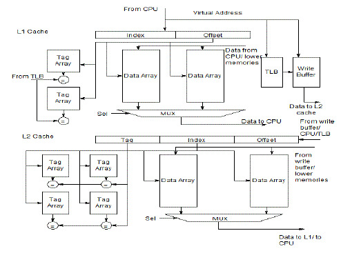
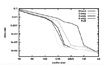
| The L1 data cache and L2 unifies cache are shown in Fig. 1 as L1 instruction cache performs reach operation only on L2 cache [11].The graph in Fig. 2 summarizes the cache performance seen on the Integer portion of the SPEC CPU2000 benchmarks, as collected by Hill and Cantin [21]. At the far right, with cache size labeled "Inf", we have the compulsory misses. If we wish to improve a machine's performance on SpecInt2000, increasing the cache size beyond 1 MB is essentially futile. That is the insight given by the compulsory misses. |
| B. Bloom Filter |
| A Bloom filter is a data structure designed to tell you, rapidly and memory-efficiently, whether an element is present in a set. The price paid for this efficiency is that a Bloom filter is a probabilistic data structure: it tells us that the element either definitely is not in the set or may be in the set. The base data structure of a Bloom filter is a Bit Vector.If the Bloom filter indicates nonexistence, then tag comparison for the cache way is avoided, thereby saving the energy that would have been consumed in tag comparison [22]. Both: 1) the smaller energy consumed to access the Bloom filter rather than the tag; and 2) the high prediction accuracy for cache way misses reduce the energy consumed in tag comparison. |
| C. Tag Comparison |
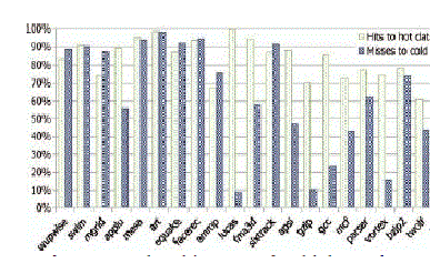
| In order to estimate whether a cache line is hot or cold, we can use a timer or counter or trace. We use the counter based method. Each cache line contains a counter which is decremented periodically. Zero at the counter indicated that the cache line is cold. Hot cache lines receive more cache hits than cold lines. If a new incoming cache reference does not go to a hot cache line, it may not go to a cold cache line as well. |
| Fig. 4 illustrates the above mentioned data. In a multistep tag comparison method, tag prediction is done by hot/cold aware cache hit prediction and pessimistic tag comparison for cold cache lines. The timeout value is proportional to the hit ratio for hot cache lines and inversely proportional to the number of tag comparisons. If the number of cold cache lines reduces, the effectiveness of early tag comparison for hot cache lines also decrease. |
PROPOSED TAG BLOOM ARCHITECTURE
|
| In this section, we present the tag-bloom architecture. We describe the implementation of way-tag modules in Section IVA. We describe the implementation of a partial tag-enhanced Bloom filter in section IV-B. We present the method for Implementation and performance details in section IV-C. |
| A. Way-Tag Modules |
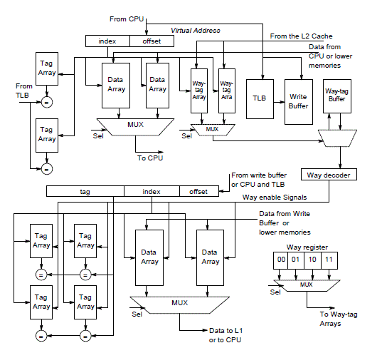
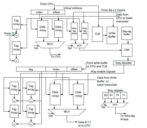
| Way-tagged cache reduces the number of ways accessed during L2 cache accesses. Locations of L1 data copies in L2 cache will not change until data is evicted from L2. When L1 data cache loads from L2, the way tag of data in L2 is also sent to L1. It is stored in a new set of way-tag arrays. These way-tags provide key info for subsequent write accesses to L2 cache. |
| Way-tag arrays are very small and the energy overhead caused can be compensated easily. Direct mapping implies only one way in the L2 cache will be activated since way-tag information of L2 cache is available i.e. from way-tag arrays, we can obtain L2 way of accessed data. Set associative implies all ways in L2 cache are activated simultaneously. |
| Components included are way-tag arrays, way-tag buffer, way decoder and way register. Way tags of each cache line in L2 cache are maintained in way-tag arrays located in L1 data cache. Way-tag buffer –buffer way tag read from way-tag arrays. Write buffer avoids write stalls when the processor waits for write operations to be completed in the L2 cache. Way-decoder decodes way tags and generate enable signal for L2 cache, activates only desired ways in L2 cache. Way register stores way tags and provide information to way-tag arrays. |
| B. Counting Bloom Filter |
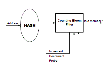
| A CBF has three operations: increment count (INC), decrement count (DEC) and test if the count is zero (PROBE) [23]. The first two operations increment or decrement the corresponding count by one, and the third one checks if the count is zero and returns true or false (single-bit output). We will refer to the first two operations as updates and to the third one as a probe. |
| A maximum-length -bit LFSR sequences through states. It goes through all possible code permutations except one. The LFSR consists of a shift register and a few embedded XNOR gates fed by a feedback loop. Each LFSR has the following defining parameters: |
| • width, or size, of the LFSR (it is equal to the number of bits in the shift register) |
| • number and positions of taps (taps are special locations in the LFSR that have a connection with the feedback loop) |
| • initial state of the LFSR which can be any value except one (all ones for XNOR feedback). |
| C. Implementation and Performance |
| The implementation of the proposed method is shown in Fig.7. It includes Tag comparison control (TC), Bloom filter (BF), Tag, Data array, Miss State Holding Register (MSHR) and write buffer. The proposed multistep tag comparison method combines both cache hit and miss prediction. The control logic for tag comparison called tag comparison control takes the input address from L1 cache and determines how many steps the tag comparison requires. It also performs the timeout countdown i.e., the tag counter update, depending on the tag comparison results. The tag counter is updated on sampled accesses in order to reduce the energy consumption for access of local TO counters. |
| By simplification of the tag comparison set, the performance is adjusted. We evaluate the energy efficiency at cache level. At processor level, smaller energy saving is obtained since L2 cache consumes only a portion of the overall energy. Reducing this overall power of a processor includes various other components like ALU, I/O, and memory and so on. It is an important research topic. |
| If the latency is smaller than lower threshold, the original configurations of the multistep tag comparison are applied. If the additional latency is larger than the upper threshold, we apply the conventional tag comparison with fixed latency of one cycle. |
EXPERIMENTAL RESULTS
|
| The simulation result of L2 cache tag-bloom architecture is obtained using XILINX ISE 8.1i with SPATAN 3E XCS500 as the target device. Simulation is also carried out in ModelSim SE 6.3f using VHDL language. The simulation result shows that the integrated tag-bloom with L2 cache is having less power compared to normal L2 cache, equal partitioned L2 cache and non-equal partitioned L2 cache approaches. The power analysis shows that the new architecture has a power consumption of 238mW which is less than the other approaches. The total equivalent gate count is also found to be lesser compared to the other approaches. Thus it is clear that the tag-bloom architecture is having 75% less power compared to the other approaches. |
| From the power and area analysis result it is clear that there is a reduction in power from 352mW to 114mW in the current environment. |
CONCLUSION
|
| In this paper, we present the tag-bloom cache architecture to increase the performance of the processor with reduced energy consumption. This proposed technique improves the accuracy of cache hit as well as cache miss prediction. This architecture attaches a tag to each way in L2 cache. These tags are stored in L1 cache while data is loaded from L2 cache. Direct mapping can be achieved during the write hits thereby reducing energy consumption. The Bloom filter checks these way tags in order to improve the accuracy of cache hit and cache miss predictions. Thus we achieve energy efficient cache architecture with no performance degradation with a minimum area overhead. This architecture can be applied to other cache operations in order to further reduce energy consumption. Future work would extend towards investigating the effectiveness of the proposed method in various other environments and extending this technique to other cache levels. |
ACKNOWLEDGMENT
|
| The authors would like to thank the Management and Principal of Sri Krishna College of Engineering and Technology, Coimbatore for providing excellent computer and library facilities and guidance. |
| |
Figures at a glance
|
 |
 |
 |
 |
| Figure 1 |
Figure 2 |
Figure 3 |
Figure 4 |
 |
 |
 |
| Figure 5 |
Figure 6 |
Figure 7 |
|
| |
References
|
- J. Maiz, S. hareland, K. Zhang, and P.Armstrong, “Characterization of multi-bit soft error events in advanced SRAMs,” in Proc. Int. Electron Devices Meeting, 2003, pp. 21.4.1–21.4.4.
- K. Osada, K. Yamaguchi, and Y. Saitoh, “SRAM immunity to cosmic-ray-induced multierrors based on analysis of an induced parasitic bipolar effect,” IEEE J. Solid-State Circuits, pp. 827–833, 2004.
- S. Segars, “Low power design techniques for microprocessors,” in Proc. Int. Solid-State Circuits Conf. Tutorial, 2001, pp. 268–273.
- Malik, B. Moyer, and D. Cermak, “A low power unified cache architecture providing power and performance flexibility,” in Proc. Int. Symp. Low Power Electron. Design, 2000, pp. 241–243.
- D. Brooks, V. Tiwari, and M. Martonosi, “Wattch: A framework for architectural- level power analysis and optimizations,” in Proc. Int. Symp.Comput. Arch., 2000, pp. 83–94.
- B. Calder, D. Grunwald, and J Emer, “Predictive sequential associative cache,” in Proc. 2nd IEEE Symp. High-Perform.Comput. Arch., 1996, pp. 244–254.
- T. N. Vijaykumar, “Reactive-associative caches,” in Proc. Int. Conf. Parallel Arch. Compiler Tech., 2011, p. 4961.
- G. Konstadinidis, K. Normoyle, S. Wong, S. Bhutani, H. Stuimer, T. Johnson, A. Smith, D. Cheung, F. Romano, S. Yu, S. Oh, V.Melamed, S. Narayanan, D. Bunsey, C. Khieu, K. J. Wu, R. Schmitt, A. Dumlao, M. Sutera, J. Chau, andK. J. Lin, “Implementation of a third-generation 1.1- GHz 64-bit microprocessor,” IEEE J. Solid-State Circuits, vol. 37, no. 11, pp. 1461–1469, Nov. 2002.
- B. Bloom, “Space/time trade-offs in hash coding with allowable errors,” Commun. ACM, vol. 13, no. 7, pp. 422–426, 1970.
- C. Zhang, F. Vahid, J. Yang, and W. Najjar, “A way-halting cache for low-energy high-performance systems,” in Proc. ISLPED, 2004, pp. 126–131.R. Panwar, and D. Rennels, “Reducing the frequency oftag compares for low power I-cache design”, In Proc. Of Int’l Symposium on Low Power Design, pages 57–62, August1995.
- K. Osada, K. Yamaguchi, and Y. Saitoh, “SRAM immunity to cosmic-ray-induced multierrors based on analysis of an induced parasitic bipolar effect,” IEEE J. Solid-State Circuits, pp. 827–833, 2004.
- C. Su and A. Despain, “Cache design tradeoffs for power and performance optimization: A case study,” in Proc. Int. Symp. Low PowerElectron.Design, 1997, pp. 63–68.
- M. D. Powell, A. Agarwal, T. N. Vijaykumar, M. Falsafi, and K. Roy, “Reducing set-associative cache energy via way-prediction and selective direct-mapping,” in Proc. Int. Symp. Microarchitecture, 2001, pp. 54–65.cvfdgv
- J.-K. Peir, S.-C.Lai, S.-L.Lu, J. Stark, and K. Lai, “Bloom filtering cache misses for accurate data speculation and prefetching,” in Proc. Supercomputing, 2002, pp. 189–198.
- M. Ghosh, E. Özer, S. Ford, S. Biles, and H.-H. S. Lee, “Way guard: A segmented counting bloom filter approach to reducing energy for setassociative caches,” in Proc. ISLPED, 2009, pp. 165–170.
- G. Keramidas, P. Xekalakis, and S. Kaxiras, “Applying decay to reduce dynamic power in set-associative caches,” in Proc. Int. Conf. High- Performance Embedded Architectures Compilers, 2007, pp. 38–53.
- R. Min, W. Jone, and Y. Hu, “Location cache: A low-power L2 cache system,” in Proc. Int. Symp. Low Power Electron.Design, 2004, pp.120–125.
- K. Inoue, T. Ishihara, and K. Murakami, “Way-predicting set-associative cache for high performance and low energy consumption,” in Proc. Int. Symp. Low Power Electron. Design, 1999, pp. 273–275.
- A.Ma, M. Zhang, and K.Asanovi, “Way memoization to reduce fetch energy in instruction caches,” in Proc. ISCA Workshop Complexity Effective Design, 2001, pp. 1–9.
- T. Ishihara and F. Fallah, “A way memoization technique for reducing power consumption of caches in application specific integrated processors,” in Proc. Design Autom. Test Euro. Conf., 2005, pp. 358–363.
- Mark D. Hill and Jasaon F. Catin, “Cache Performance for SPEC CPU2000 Benchmarks,” Cs.wisc.edu.Retrieved 2010-05-02.
- Hyunsun Park, SungjooYoo and Sunggu Lee, “A Multistep Tag Comparison Method for a Low-Power L2 Cache,” IEEE transactions on Computer- Aided Design of Integrated Circuits and Systems, Page 559-572, Vol. 31, No. 4, April 2011.
- Elham Safi, Andreas Moshovos, Andreas Veneris, “ L-CBF: A Low-Power, Fast Counting Bloom Filter Architecture,” in Proc. IEEE Transactions on VLSI Systems, Vol. 16, No. 6, June 2008.
|