Keywords
|
| Frequency control, interleaved flyback, light emmiting diode (LED), power factor correction (PFC),total harmonic distortion(THD). |
INTRODUCTION
|
| Due to the high increase in recital that High Brightness Light Emitting Diodes (HB-LEDs) have been developing in the recent years, they have become an interesting and overcoming choice in most cases for general lighting solutions. In addition to their innate high efficiency, there is no mercury inside the devices and they carry out an extremely long operating life. The main purpose of this paper consists of presenting a topology for running LED streetlights from an Ac source. |
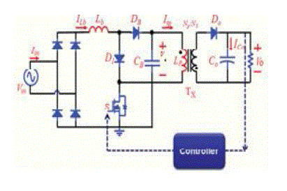
| In a single-stage approach, input-current shaping, isolation, and high-bandwidth control are performed in a single step, i.e., without creating a transitional dc bus. Among the single-stage circuits, a number of circuits described in seem particularly striking because they can be implemented with only one semiconductor switch and a simple control. All these single stage, single-switch input-current shaping (S41CS) circuits[3] integrate the boostconverter front end with the forward converter or the flyback-converter dc/dc stage. Fig. 1 shows the flyback converter .The two additional primary windings, NI and N2, are employed to keep the voltage of energy-storage (bulk) capacitor below a desired level in the entire line and load ranges. Boost inductor can function either in the discontinuous conduction mode (DCM) or in the continuous conduction mode (CCM). Generally, the CCM operation offers a slightly higher efficiency compared to the DCM operation. However, the DCM operation gives a less total harmonic distortion (THD) of the line current compared to that of the CCM operation. |
| When the flyback transformer in operates with a DCM magnetizing current, the switch voltage during the off time after the magnetizing current decreases to zero oscillates around with an amplitude equal to Nvo because of the resonance between the magnetizing inductance of the transformer and the output capacitance of the switch. Therefore, the flyback converter operating with a DCM magnetizing current of the transformer also suffers from capacitive-discharging turn-on switching loss Po,,,(,).The maximum PON in a DCM flyback converter is the same as the PoN in A ccm flyback converter. Single-Stage PFC is generally an AC/DC converter with inherent power factor correction function.[1]The energy storage capacitor is necessary in the Single-Stage PFC, which is used to buffer the variation between the instantaneous input power and the output power. Conventionally, a bulk electrolytic capacitor is used to build the single-stage PFC achieves good power factor and tight output voltage regulation. With limited lifetime from the electrolytic capacitor, which is normally in the vicinity of couple thousands hours under rated condition, the lifetime of the state-of-the-art LED power supply is far away from the expectation from LED[5]. |
| LEDs can only be driven by dc voltage, and thus, an ac-to-dc conversion stage is necessary. Among the acto- dc driving circuits for LEDs, switching converter is one of the most all the rage and economical driving solutions. Conventional ac-to-dc switching converters are composed of a bridge-diode rectifier followed by a bulk capacitor and a dc-to-dc switching converter; this topology is inherently vulnerable to poor performances in power factor (PF) and harmonic distortion. In order to fulfill with the regulations on current harmonics and improve the PF, an additional PF corrector (PFC) stage is cascaded in front of the traditional converter. Inspite of its good performance, such two-stage solutions are usually more expensive and energy inefficient. For general lighting application, there are several regulations. Being required by the Energy-Stare, the input current power factor should be higher than 0.9[6]. To meet those regulations, the LED power Supply should have the power factor correction (PFC) ability. Power factor correction can be achieved either by passive circuit or by an active circuit. Due to the disadvantage of low power factor, high THD and bulky size, passive PFC is not a good candidate. Comparing to the Two-Stage PFC, Single-Stage PFC has the advantages: simple circuit configuration, easy control implementation and For the sake of reducing the cost and improving the efficiency, single-stage converter circuits have been developed. Although these single-stage converters have many advantages, their efficiencies are usually not good enough(about 80%). On the other hand, for safety considerations, isolated ac-to-dc converters are more popular among the LED driving circuits. However, the efficiency is remarkably encumbered with the leakage inductance when applying isolated transformers. To solve these drawbacks, this paper proposes a novel single-stage high-PF ac-to-dc LED driving circuit with a leakage inductance energy recycling mechanism[7−8]. |
| The main advantageous point of the newly-proposed PFC converter includes that the output DC output voltage ripple factor can be minimized by using two channel pulse modulation control loops. In addition, the active PFC converter treated here can also effectively suppress the line current harmonics in utility AC grid without any specific feedback control scheme employing a current sensor interface circuit. |
OVERVIEW OF TWO STAGE STRUCTURE
|
| In the general lighting applications with low power, Single-Stage PFC is widely used. An interleaved flyback–forward boost converter is proposed in this paper. The switched capacitors are used to realize the controllable voltage source function and balance the currents of the interleaved two phases without an additional current-sharing module. Voltage lift function of the switched capacitor also reduces the turns ratio of the transformers and alleviates the voltage stresses of the output diodes. |
| As the transformers operate in flyback and forward modes alternately, part of the output energy is stored in the switched capacitors; therefore, the size of magnetic components can be reduced. Since the current falling rates of the clamping and output diodes, when they turn off, are controlled by the leakage inductance, the diode reverserecovery problem is alleviated. Active clamp circuits are applied for the interleaved two phases to recycle the leakage energy and absorb the voltage spikes caused by the leakage inductance. A CRM fly back converter is widely used as the single-stage structure due to its high efficiency by valley switching even if it still shows poor PF and THD under light load condition due to the valley switching of the CRM control method. On the other hand, a DCM flyback converter shows good PF and THD, but it has low efficiency due to its high rms current. |
| Most single-stage flyback converters are hard to apply at over 60–70W LED applications, because the flyback converter usually has low efficiency and a huge transformer with high power applications. To handle high output power with the flyback topology, an interleaving control method is a possible solution. The interleaving control method provides small input and output filters, low voltage stress on the main switch and a low profile design when compared to non interleaving methods. While the CRM interleaved flyback converter has high efficiency, but shows poor PF and THD under light load condition, the discontinuous conduction mode (DCM) interleaved flyback converter has good PF and THD under light load condition, but shows low efficiency due to its high rms current. |
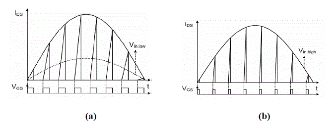
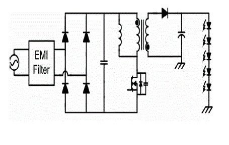
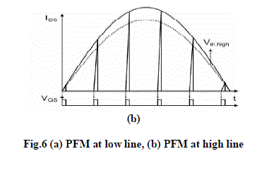
| In two stage structure- CRM flyback converter is used. Critical conduction mode(CRM) control is a control strategy in which the active switch turns on when the inductor current falls into zero point to remove the freewheeling diode reverse recovery. This control operates on the boundary condition between continuous conduction mode(CCM) and discontinuous conduction mode(DCM) with variable switching frequency. In conventional method constant duty cycle of 0.5, the constant frequency PWM method and the proposed method at low and high ac lines, the conventional PFM method shows the disadvantage of a large frequency variation between low and high ac lines. It causes severe switching loss at high ac line. The frequency variation between the low and high lines is obtained. |
| DISADVANTAGES |
| 1. The two-stage structure needs a large number of components are used. |
| 2. Two kinds of control ICs so that it costs a lot. |
| 3. It shows low efficiency due to the two processes of the input power. |
| 4. CRM boost converter for PFC, it shows poor PF and THD under light load condition due to the negative drain current for valley switching. |
| 5. Two-stage structure cannot cover the wide output power range of LED lighting applications. |
PROPOSED SYSTEM
|
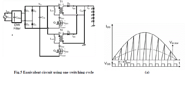
| In this paper Single stage structure is used to achieve high efficiency, improved PF and THD in wide output power range, this paper proposes a pulse duty cycle pulse frequency modulation (PDPFM) control method for an interleaved single-stage flyback (ISSF) converter. |
| The proposed control method adopts DCM operation which can achieve high PF for wide output power range. In the proposed method, the interleaved DCM flyback converter is basically controlled by frequency modulation, not pulse width modulation. The turn-ON time corresponds to the switching frequency to reduce the frequency variation and to achieve high efficiency |
| Ton = m ãÃÆûfsw ….(1) |
| Where m is a constant. For low conduction loss under heavy load with low ac line condition, the proposed method increases the switching frequency and the turn-ON time. On the other hand, to reduce the switching loss under light load with high ac line, the proposed method decreases both the switching frequency and the turn-ON time. Therefore average output power over half of the ac line period can be expressed as |
| Po = η ãÃÆûV ^2lineãÃÆûm ãÃÆûD ãÃÆûFsw âÃËÃâ¢Lm1 ….(2) |
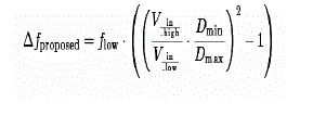
| Where V line is the ac line voltage in rms, η is efficiency, D is duty cycle, and Lm1 equals Lm2 Output power is controlled by duty cycle and switching frequency. As a result, the proposed converter can achieve high PF and low THD by utilizing DCM operation, and high efficiency due to frequency modulation in wide output power range. The frequency calculation between low line and high lines can be expressed as |
 |
CIRCUIT DESCRIPTION
|
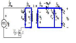
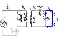
| Equivalent circuit with interleaved connection.In here rectifying diodes converts AC to DC and input DC supply is given to primary windings.Fig 5(a) and (b) shows the modified technique involved in it. |
| A. MODES OF OPERATION : |
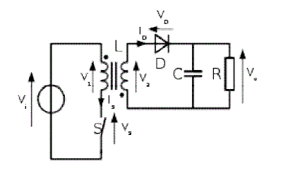
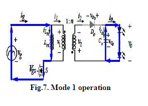
| When switch ‘S’ is on, the primary winding of the transformer gets connected to the input supply with its dotted end connected to the positive side. At this time the diode ‘D’ connected in series with the secondary winding gets reverse biased due to the induced voltage in the secondary. Thus with the turning on of switch ‘S’, primary winding is able to carry current but current in the secondary winding is blocked due to the reverse biased diode. The flux established in the transformer core and linking the windings is entirely due to the primary winding current. This mode of circuit has been described here as Mode-1 of circuit operation. The current carrying part of the circuit and shows the circuit that is functionally equivalent to the fly-back circuit during mode-1. |
| Mode-2 of circuit operation starts when switch ‘S’ is turned off after conducting for some time. The primary winding current path is broken and according to laws of magnetic induction, the voltage polarities across the windings reverse. Reversal of voltage polarities makes the diode in the secondary circuit forward biased. The current path during mode-2 of circuit operation while the functional equivalent of the circuit during this mode primary winding current is interrupted due to turning off of the switch ‘S’, the secondary winding immediately starts conducting such that the net mmf produced by the windings do not change abruptly. Continuity of mmf, in magnitude and direction, is automatically ensured as sudden change in mmf is not supported by a practical circuit for reasons briefly given below. Sudden change in flux will mean sudden change in the magnetic field energy and this in turn will mean infinite magnitude. The secondary winding, while charging the output capacitor starts transferring energy from the magnetic field of the fly back transformer to the power supply output in electrical form. If the off period of the switch is kept large, the secondary current gets sufficient time to decay to zero and magnetic field energy is completely transferred to the output capacitor and load. Flux linked by the windings remains zero until the next turn-on of the switch, and the circuit is under discontinuous flux mode of operation. Alternately, if the off period of the switch is small, the next turn on takes place before the secondary current decays to zero. The circuit is then under continuous flux mode of operation. |
| During discontinuous mode, after complete transfer of the magnetic field energy to the output, the secondary winding emf as well as current fall to zero and the diode in series with the winding stops conducting. The output capacitor however continues to supply uninterrupted voltage to the load. This part of the circuit operation has been referred to as Mode-3 of the circuit operation. |
| Mode-3 ends with turn ON of switch ‘S’ and then the circuit again goes to Mode-1 and the sequence repeats. Fig.9 respectively shows the current path and the equivalent circuit during mode-3 of circuit operation. The voltage and current waveforms of the winding over a complete cycle. It may be noted here that even though the two windings of the fly-back transformer don’t conduct simultaneously they are still coupled magnetically (linking the same flux) and hence the induced voltages across the windings are proportional to their number of turns. |
POWERFACTOR CORRECTION
|
| Power factor correction brings the power factor of an AC power circuit closer to 1 by supplying reactive power of opposite sign, including capacitors or inductors that proceed to eliminate the inductive or capacitive effects of the load, respectively. In the electricity industry, inductors are said to munch through reactive power and capacitors are said to supply it, even though the energy is just moving back and into view on each AC cycle. |
1) Distortion power factor
|
| The distortion power factor describes how the harmonic distortion of a load current reduces the average power transferred to the load. |
| Distortion powerfactor=1/(1+THDi^2)^1/2 …(4) |
| THD is the total harmonic distortion of the load current. It can abridged by low ac line voltage, usually in low ac line, the input current is take away distorted due to high drain current. |
| Efficiency can be enhanced by variable switching frequency, turn on time and duty cycle |
EXPERIMENTAL RESULTS
|
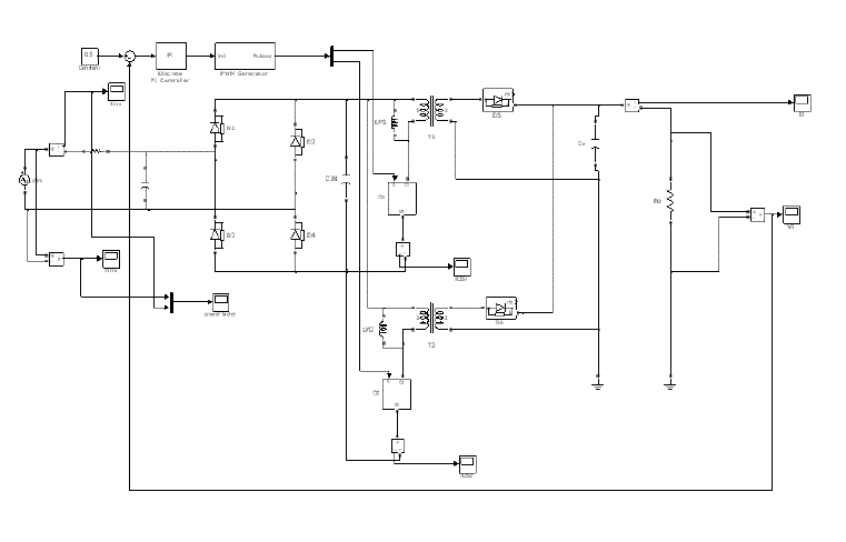
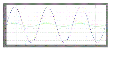
| The operation of the proposed converter has been analyzed by MATLAB /SIMULINK.Table 1 shows prototype specifications of the proposed interleaved single stage flyback converter at the LED load of 3V,300mA respectively. |
| The LED units are configured in series varies according to LED applications, the range of output voltage is wide. |
CONCLUSION
|
| The PDPFM control method for an ISSF converter has been proposed. The control method increases the switching frequency, the turn-ON time and the duty cycle under heavy load with low ac line condition for low rms current and it decreases under light load with high ac line condition for low switching loss. At 100% load condition it can achieve 0.998 power factor and efficiency upto 90−92%.The proposed converter has higher peak current than the conventional converters at high ac line condition. The proposed converter has high efficiency, better PF, and low THD. Therefore, the proposed converter is considerably suitable for wide output range LED application |
Tables at a glance
|
 |
 |
| Table 1 |
Table 2 |
|
Figures at a glance
|
 |
 |
 |
 |
 |
| Figure 1 |
Figure 2 |
Figure 3 |
Figure 4 |
Figure 5 |
 |
 |
 |
 |
 |
| Figure 6 |
Figure 7 |
Figure 8 |
Figure 9 |
Figure 10 |
 |
 |
| Figure 11 |
Figure 12 |
|
References
|
- Y.-C. Chuang,Y.-L.Ke, H.-S. Chuang, and C.-C.He, “Single-stage power factor- correction circuit with flyback converter to drive LEDs forlighting applications,” in Proc. IEEE Ind. Appl. Soc. Annu. Meeting, 2010, pp. 1–9.
- R. Redl and L. Balogh, “Design considerations for single-stage isolated power-factor-corrected power supplies with fast regulation of theoutput voltage,” in Proc. IEEE Appl. Power Electron.Conf., 1995, vol. 1, pp. 454– 458.
- L. Huber and M. M. Jovanovic, Single-stage single-switch input current shaping technique with reduced switching loss,” IEEE Trans.Power Electron., vol. 15, no. 4, pp. 681–687, Jul. 2000.
- K.-H.Liu and Y.-L.Lin, “Current waveform distortion in power converters,”inProc. IEEE Power Electron. Spec. Conf., 1989, pp. 825–829.
- D. Gacio, J. M. Alonso, A. J. Calleja, J. Garcia, and M. R. Secades,“A universal-input single-stage high-power-factor power supply forHBLEDs based on integrated buck-flyback converter,” IEEE Trans. Ind. Electron.,vol. 58, no. 2, pp. 589–599, Feb. 2011.
- J. A. Villarejo, J. Sebastian, F. Soto, and E. de Jodar, “Optimizing the design of single-stage power-factor correctors,” IEEE Trans. Ind.Electron.,vol. 54, no. 3, pp. 1472–1482, Jun. 2007.
- V. F. Pires and J. F. Silva, “Single-stage double-buck topologies with high power factor,” J. Power Electron., vol. 11, no. 5, pp. 655–661,Sep. 2011.
- F. Tao and F. C. Lee, “An interleaved single-stage power-factor-correction electronic ballast,” in Proc. IEEE Appl. Power Electron. Conf.,2000,vol. 1, pp. 617–623.
- J. Zhang, F. C. Lee, and M. M. Jovanovic, “A novel interleaved discontinuous-current-mode single-stage power-factor-correction techniquewith universal-line input,” in Proc. IEEE Power Electron. Spec.Conf., 2001, vol. 2, pp.1007–1012.
- J.Uceda, "Novel power factor correction AC/DC converters with high efficiency based on the forward topology" IEEE International PowerElectronics Specialists Conference, Vol.2, pp.1815, 1998.
- R. Erickson, M. Madigan ,S. Singer. “Design of a Simple High-Power-Factor Rectifier Based on the Flyback converter”. IEEE PowerElectronics Specialists Conference 1990. pp. 792-801
- K. I. Hwu and Y. T. Yau, “An interleaved AC-DC converter based on current tracking,” IEEE Trans. Ind. Electron., vol. 56, no. 5, pp.1456– 1463, May 2009.
- J. Sun, D. M. Mitchell, M. Greuel, P. T. Krein, and R. M. Bass, “Averaged modeling of PWM converters operating in discontinuousconduction mode,” IEEE Trans. Power Electron., vol. 16, no. 4, pp. 482–492, Jul. 2001.
- J. Sebastian and J. Uceda, “The double converter: A fully regulated two output dc-dc converter,” IEEE Trans. Power Electron., vol. PE-2,no. 3, pp. 239–246, Jul. 1987.
- H. H. Seong, D. J. Kim, and G. H. Cho, “A new ZVS DC/DC converter with fully regulated dual outputs,” in Proc. IEEE Power Electron.Spec.Conf., 1993, pp. 351–356.
- H. E. Tacca, “Single-switch two-output flyback-forward converter operation,”IEEE Trans. Power Electron., vol. 13, no. 5, pp. 903–911,Sep.1998.
- Y. Chen and Y. Kang, “A fully regulated dual-output dc-dc converter with special-connected two transformers (SCTTs) cell andcomplementary pulse width modulation-PFM (CPWM-PFM),” IEEE Trans. Power Electron., vol. 25, no. 5, pp. 1296–1309, May 2010.
- Tamyurek and D. A. Torrey, “A three-phase unity power factor single stage AC-DC converter based on an interleaved flyback topology,”IEEE Trans. Power Electron., vol. 26, no. 1, pp. 308–318, Jan. 2011.
- F. Yang, X. Ruan, Y. Yang, and Z. Ye, “Interleaved critical current mode boost PFC converter with coupled inductor,” IEEE Trans. PowerElectron.,vol. 26, no. 9, pp. 2404–2413, Sep. 2011.
- S. Park, Y. Park, S. Choi, W. Choi, and K. B. Lee, “Soft-switched interleaved boost converters for high step-up and high-powerapplications,” IEEE Trans. Power Electron., vol. 26, no. 10, pp. 2906–2914, Oct. 2011.
- Y. Hu, L. Huber, and M. M. Jovanovic, “Single-stage, universal-input AC/DC LED driver with current-controlled variable PFC boostinductor,”IEEE Trans. Power Electron., vol. 27, no. 3, pp. 1579–1588, Mar. 2012.J. Turchi, “Power factor correction stages operated incritical conduction mode,” ON Semiconductor, Phoenix, AZ, Appl. Note no. AND8123/D,2003.
|