Keywords
|
| PV module, Power conditioning system, Voltage mode control, Level shifted sinusoidal pulse width modulation(FPGA). |
INTRODUCTION
|
| Solar energy, at present has proved to be one of the best alternatives to overcome the drawbacks of the conventional energy sources like pollution, degradation of fossil fuels etc. to meet the load requirements [1]. In addition to this, Solar energy source has its own advantages like highly modular, longer life with little maintenance, high power capability per unit of weight and highly mobile and portable. |
| Solar PV cell is a basic element in solar PV system which converts light energy into electrical energy. Combination of several PV cells together forms Solar PV Module [2]. This will produce variable DC output voltage with the inputs of solar irradiation and temperature. Under normal operating condition, it operates at a unique operating point to produce maximum output power. We can easily obtain maximum efficiency by using Maximum Power Point Tracker (MPPT), which is a part of power conditioning system. Power Conditioning System (PCS) is a part of power electronic system used to manage the electrical energy effectively and to provide high quality maximum power from solar PV modules [3]. Boost DC-DC converter is used to get desired high level DC output voltage from variable low level DC power supply. Diode Clamped 3-level inverter is used to get good quality of 3-Phase AC voltage to feed 3-Phase loads from the fixed DC voltage. Diode Clamped 3-level Inverter offers some advantages like lower THD, lower dv/dt, less common mode voltage, high switching frequency and high input power factor. |
| The proposed PV system comprises of 2-stage power conversion using FPGA. The first stage converts the variable DC voltage obtained from solar PV module/array into fixed DC using Boost converter [4]. In the second stage of power conversion, the output of the first stage is fed to 3-phase, 3- level Diode clamped Inverter. |
| In the proposed PV system, 100watts solar PV module is used to feed closed loop DC-DC Boost converter to drive Diode Clamped 3-Level Inverter. Voltage Mode control (VMC) technique has been employed to control the Boost Converter. Type- 3 error amplifier is designed to meet practical stability margins and used as compensator for Boost converter. In this paper, 2-stage Power conditioning system is controlled with the help of digital controller (FPGA) [5]. Simulations of the proposed PV system have been done at 0.8pf of 3-phase inductive load and observed that the THD of this system is 1.73%. |
PROPOSED PV SYSTEM
|
| We know that the solar PV system is the combination of several elements like PV module, Power conditioning elements and load. |
| The main elements which have been presented in the proposed system are explained in detail in next chapters. Block diagram representation of 2-stage power conditioning PV system is shown in above fig.1. |
A. PV Cell :
|
| Figure 3 shows us a simple equivalent circuit for the practical solar cell model. Similarly the working methodology of PV cell is represented by figure 4. , where electrons and holes move across the PN junction to form electron- hole pairs which in turn generates the energy depending upon the solar radiation and temperature. |
B. Power conditioning system:
|
| Power Conditioning System is branch of power electronics, which are used to describe the management of electrical energy effectively, tracks the maximum operating point and provide good quality of desired AC output. |
| Switch Mode power Converter has many advantages compared to linear switching regulator. Power conditioning Elements should have modern and sophisticated electronic devices. Since PV Systems cost is relatively high as compared to other energy source systems, in order to meet optimized cost of PV system, it is suggested to use high efficiency power conditioning elements. DC-DC converters are used to design for tracking maximum power from the solar panels and step up/down the available DC voltage from PV panels. MPPT technique minimizes the amount of power dissipated and helps to extract the maximum power available. |
C. DC- DC Boost Converter:
|
| DC- DC Boost Converter converts low level DC voltage to high level DC voltage. DC-DC Boost converter normally operates either in continuous conduction mode or in discontinuous conduction mode. In the proposed power conditioning system, the boost converter operates in Continuous Conduction Mode (CCM) as shown in figure 5. |
| In CCM, power can be transferred from source to load using 2 step processes. When the switch 'S' is turned ON, inductor stores the energy and its equivalent circuit is shown in figure 6. When the switch 'S' is turned OFF, energy stored in the inductor and supply energy is transferred to the load through the diode and its equivalent circuit is shown in figure 7. Equivalent waveforms of voltage across an inductor, current through inductor, current through diode and capacitor current are shown in figure 8. |
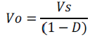
| For an ideal DC-DC Boost Converter, the relation between input voltage and load voltage is given by |
 |
| To obtain desired regulated output voltage from the dc-dc boost converter which feeds to inverter, double lead integral controller is designed to achieve minimum closed loop stability margins. The block diagram of closed loop feedback dc-dc boost converter is shown in figure 9. |
| Pulse width modulator Tm compares the fixed frequency saw-tooth voltage Vsaw with the control voltage and produces the required duty ratio D. The DC-DC Boost converter plant Tp(s) gives desired output voltage VMLI corresponding to the corrected duty ratio produced by modulator. The double lead integral controller which produces control voltage Vo has been designed and implemented on FPGA spartan-3 XS3C5000. |
D. Diode Clamped 3-Level Inverter:
|
| 3-Level Diode Clamped inverter is used as one of the devices in power conditioning system to convert regulated DC voltage into 3-Phase AC voltage to drive 3- phase loads which is shown in figure 10. To clamp the switch voltage to half the level of the dc-dc converter voltage, diodes are placed between the neutral point and the midpoint of the MOSFETs. The voltage arrived from the closed loop boost DC-Dc converter is split into 2 voltage levels by using 2 - capacitor which are connected in series and placed across the boost converter output terminals. The midpoint of the two capacitors is treated as the neutral point. |
| The 3-level Diode Clamped Inverter output voltage has three states: Vdc/2, 0, and -Vdc/2. To get the voltage level ofVdc/2, switches M1 and M2need to be switched on; for -Vdc/2, switches M3 and M4 need to be switched on; and for the zero level, switches M2 and M3need to be switched on. When both Ml and M2 turned on, the voltage across terminal 'a' and '0' point is Vdc, i.e.,Vao = Vdc. In this case clamping Diodes balances out the voltage sharing between M3 and M4,with M3 blocking the voltage across Cs1 and M4 blocking the voltage across Cs2. Observe that output phase voltage Van is ac, voltage between terminal 'a' and '0' (Va0) is dc and the difference between phase voltage Van and Va0is the voltage across Cs2, which is Vdc/2. |
| A level shifted sinusoidal pulse width modulation scheme is employed as an open loop control strategy to control the diode clamped 3-level inverter. In this scheme, the gate pulses for each phase MOSFETs can be generated by comparing fixed two carrier signals of carrier switching frequency with the reference sinusoidal voltage of line frequency. This control technique is also employed on FPGA to generate gate pulses |
CONCLUSION
|
| This paper presents the complete analysis of novel 2-stage power conditioning system for PV power by the help MATLAB simulation environment. The current THD of 3-level diode clamped inverter is found to be 1.34% at 0.8 pf for inductive loads. Compared to the conventional PV systems, the value obtained from the proposed system is highly appreciable. The FPGA system implementation for Boost converter has helped to generate the good quality pulses which makes the proposed system effective and efficient for the application with the 3-phase AC loads. |
Figures at a glance
|
 |
 |
 |
 |
 |
| Figure 1 |
Figure 2 |
Figure 3 |
Figure 4 |
Figure 5 |
 |
 |
 |
 |
 |
| Figure 6 |
Figure 7 |
Figure 8 |
Figure 9 |
Figure 10 |
 |
 |
 |
 |
 |
| Figure 11 |
Figure 12 |
Figure 13 |
Figure 14 |
Figure 15 |
 |
| Figure 16 |
|
References
|
- Middlebrook R. D, “Transformerless DC-to-DC converters with large conversion ratios,” IEEE Trans. PowerElectronics, vol.3, no.4, pp.484-488, Oct 1988.
- ZhihongBai; Zhongchao Zhang; Yao Zhang; , "A Generalized Three-Phase Multilevel Current Source Inverter with Carrier Phase- Shifted SPWM," Power Electronics Specialists Conference, 2007. PESC 2007.IEEE ,vol.,no., pp.2055-2060, 17-21 June 2007 doi: 10.1109/PESC.2007.4342322
- J. Rodriguez, J.-S. Lai, and F.Z.Peng, “Multilevel inverters: A survey of topologies, controls, and applications,” IEEE Trans. Ind. Electron., vol. 49, no. 4, pp. 724–738, Aug. 2002.
- S. Ali Khajehoddin, AlirezaBakhshai, and Praveen Jain,”TheApplication of the Cascaded Multilevel converters in Grid Connected Photovoltaic Systems”, IEEE Canada Electrical Power Conference, 2007
- FredeBlaabjerg, Remus Teodorescu, Zhe Chen and Marco Liserre ,”Power Converters and Control of Renewable Energy Systems” ,IEEE Journal.
|