The increase of the Integrated Circuit (IC) capabilities offers the designer the possibility to include more complex functionality into it. Processors are one of the general purpose modules found in these complex circuits which can be reused for test. It has been shown that processors can reach similar levels of Fault Coverage (FC) to LFSR, by looping arithmetic operations. Weighted pseudorandom techniques have also been used to improve the fault coverage. These weighted pseudorandom techniques result in low testing time and power. Generation of test vectors using arithmetic functions is becoming an attractive solution due to possibility of reusing internal arithmetic data paths of system cores for testing purposes. It requires neither additional IC area nor special bus to transmit test vectors; these can be sent by standard address or data buses to the Modules Under Test (MUT). Of the four basic arithmetic operations that are available in processors, addition has the most advantages: it is usually implemented by hardware, and it is more energy and time efficient. Also, if the buses require the The increase of the Integrated Circuit (IC) capabilities offers the designer the possibility to include more complex functionality into it. Processors are one of the general purpose modules found in these complex circuits which can be reused for test. It has been shown that processors can reach similar levels of Fault Coverage (FC) to LFSR, by looping arithmetic operations. Weighted pseudorandom techniques have also been used to improve the fault coverage. These weighted pseudorandom techniques result in low testing time and power. Generation of test vectors using arithmetic functions is becoming an attractive solution due to possibility of reusing internal arithmetic data paths of system cores for testing purposes. It requires neither additional IC area nor special bus to transmit test vectors; these can be sent by standard address or data buses to the Modules Under Test (MUT). Of the four basic arithmetic operations that are available in processors, addition has the most advantages: it is usually implemented by hardware, and it is more energy and time efficient. Also, if the buses require thetransmission of the test vector by pieces, it can be split into smaller operations by propagating the carry signal. This project proposes a method for designing a low power and area efficient test pattern generator (TPG) using ALU. The TPG is designed using a newly proposed Carry Select Adder in place of the binary adders in ALU. This helps to achieve low power consumption , low area and less speed too than the earlier designs.
Keywords |
| TPG, MUT, LFSR, Newly Proposed
Carry Select Adder. |
INTRODUCTION |
| Pseudorandom built-in self test (BIST)
generators have been widely utilized to test integrated
circuits and systems. The arsenal of pseudorandom generators includes, among others, linear feedback shift
registers (LFSRs), cellular automata [2], and
accumulators driven by a constant value . For circuits
with hard-to-detect faults, a large number of random
patterns have to be generated before high fault coverage
is achieved. Therefore, weighted pseudorandom
techniques have been proposed where inputs are biased
by changing the probability of a “0” or a “1” on a given
input from 0.5 (for pure pseudorandom tests) to some
other value . |
| Weighted random pattern generation methods
relying on a single weight assignment usually fail to
achieve complete fault coverage using a reasonable
number of test patterns since, although the weights are
computed to be suitable for most faults, some faults may
require long test sequences to be detected with these
weight assignments if they do not match their activation
and propagation requirements. Multiple weight
assignments have been suggested for the case that
different faults require different biases of the input
combinations applied to the circuit, to ensure that a
relatively small number of patterns can detect all faults.
Approaches to derive weight assignments for given
deterministic tests are attractive since they have the
potential to allow complete coverage with a significantly
smaller number of test patterns. |
| In order to minimize the hardware
implementation cost, other schemes based on multiple
weight assignments utilized weights 0, 1,and 0.5. This
approach boils down to keeping some outputs of the
generator steady (to either 0 or 1) and letting the
remaining outputs change values (pseudo-) randomly
(weight 0.5). This approach, apart from reducing the
hardware overhead has beneficial effect on the consumed
power, since some of the circuit under test (CUT) inputs
(those having weight 0 or 1) remain steady during the
specific test session. |
| Current VLSI circuits, e.g., data path
architectures, or digital signal processing chips
commonly contain arithmetic modules [accumulators or
arithmetic logic units (ALUs)]. This has fired the idea of
arithmetic BIST (ABIST) . The basic idea of ABIST is to
utilize accumulators for built-in testing (compression of
the CUT responses, or generation of test patterns) and
has been shown to result in low hardware overhead and
low impact on the circuit normal operating speed.
Manich et al. presented an accumulator-based test
pattern generation scheme that compares favorably to
previously proposed schemes.It was proved that the test
vectors generated by an accumulator whose inputs are
driven by a constant pattern can have acceptable
pseudorandom characteristics, if the input pattern is
properly selected.However, modules containing hard-todetect
faults still require extra test hardware either by
inserting test points into the mission logic or by storing
additional deterministic test patterns . |
| In order to overcome this problem, an
accumulator-based weighted pattern generation scheme
was proposed. The scheme generates test patterns having
one of three weights, namely 0, 1, and 0.5 therefore it
can be utilized to drastically reduce the test application
time in accumulator-based test pattern generation.
However, the scheme proposed possesses three major
drawbacks: 1) it can be utilized only in the case that the
adder of the accumulator is a ripple carry adder; 2) it
requires redesigning the accumulator; this modification,
apart from being costly, requires redesign of the core of
the datapath, a practice that is generally discouraged in
current BIST schemes; and 3) it increases delay, since it
affects the normal operating speed of the adder.In the
base paper a novel scheme for the weighted pattern
generation which does not impose any condition on the
adders used was studied. |
| In this paper a novel scheme for the design of low
power and area efficient test pattern generator using
ALU is proposed. This paper is organized as follows. In
Section II, the idea underlying the accumulator-based 3-
weight generation is presented. In Section III, the design
methodology to generate the 3-weight patterns utilizing
an accumulator is presented. In section IV the results
have been compared. |
ACCUMULATOR-BASED 3-WEIGHT
PATTERN GENERATION |
| We shall illustrate the idea of an accumulatorbased
3-weight pattern generation by means of an example. Let us consider the test set for the c17 ISCAS
benchmark [12], [31] given in Table I. Starting from this
deterministic test set, in order to apply the 3-weight
pattern generation scheme, one of the schemes proposed
in [5], [8], and [9] can be utilized. According to these
schemes, a typical weight assignment procedure would
involve separating the test set into two subsets, S1 and
S2 as follows: S1={T1, T4},S2 ={T2 ,T3}. |
| The weight assignments for these subsets is
W{S1} ={_,_,1,_,1} and W{S2} = {_,_,0,1,0} , where a
“_” denotes a weight assignment of 0.5, a “1” indicates
that the input is constantly driven by the logic “1” value,
and “0” indicates that the input is driven by the logic “0”
value. In the first assignment, inputs A[2] and A[0] are
constantly driven by “1”, while inputs A[4], A[3], A[1]
are pseudo randomly generated (i.e., have weights 0.5).
Similarly, in the second weight assignment (subset S2),
inputs A[2] and A[0] are constantly driven by “0”, input
A[1] is driven by “1” and inputs A[4] and A[3] are
pseudo randomly generated. |
| The above reasoning calls for a configuration
of the accumulator, where the following conditions are
met: 1) an accumulator output can be constantly driven
by “1” or “0” and 2) an accumulator cell with its output
constantly driven to “1” or “0” allows the carry input of
the stage to transfer to its carry output unchanged. This
latter condition is required in order to effectively
generate pseudorandom patterns in the accumulator
outputs whose weight assignment is “_”. |
DESIGN METHODOLOGY |
| The implementation of the weighted-pattern
generation scheme is based on the full adder truth table,
presented in Table II. From Table II we can see that in
lines #2, #3, #6, and #7 of the truth table,Cout=Cin.
Therefore, in order to transfer the carry input to the carry
output, it is enough to set A[i] = not B[i]. The proposed
scheme is based on this observation. |
| The implementation of the proposed weighted
pattern generation scheme is based on the accumulator
cell presented in Fig. 1, which consists of a Full Adder
(FA) cell and a D-type flip-flop with asynchronous set
and reset inputs whose output is also driven to one of the
full adder inputs. In Fig. 1, we assume, without loss of
generality, that the set and reset are active high signals.
In the same figure the respective cell of the driving
register B[i] is also shown. For this accumulator cell, one
out of three configurations can be utilized, as shown in
Fig. 2. |
| In Fig. 2(a) we present the configuration that
drives the CUT inputs when A[i]=1 is required.Set[i]=1
and Reset[i] = 0 and hence A[i]=1 and B[i] =0. Then the
output is equal to 1, and Cin is transferred to Cout. |
| In Fig. 2(b), we present the configuration that
drives the CUT inputs when A[i]=0 is required. Set[i]=0 and Reset[i] = 1 and hence A[i]=0 and B[i]=1. Then, the
output is equal to 0 and Cin is
transferred to Cout. |
| In Fig. 2(c), we present the configuration that
drives the CUT inputs when A[i]= _ is required. Set[i]=0
and Reset[i] = 0.The D input of the flip-flop of register B
is driven by either 1 or 0, depending on the value that
will be added to the accumulator inputs in order to
generate satisfactorily random patterns to the inputs of
the CUT. |
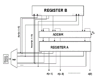
| In Fig. 3, the general configuration of the
proposed scheme is presented.The Logic module
provides the Set[n-1:0] and Reset[n-1:0] signals that
drive the S and R inputs of the Register A and Register B
inputs. Note that the signals that drive the S inputs of the
flip-flops of Register A, also drive the R inputs of the
flip-flops of Register B and vice versa.
In the figure 2 , the performance of the circuit is
increased by using a modified carry select adder as
follows. |
MODIFIED CSLA USING BEC |
| The Binary to excess one Converter (BEC) replaces
the ripple carry adder with Cin=1, in order to reduce the
area and power consumption of the regular CSLA. The
modified16-bit CSLA using BEC is shown in Fig. 4 [1].
The structure is again divided into five groups with
different bit size RCA and BEC.The group 2 of the
modified 16-bit CSLA is shown Fig. 5. By manually
counting the number of gates used for group 2 is 43 (full
adder, half adder, multiplexer, BEC).One input to the
mux goes from the RCA with Cin=0 and other input
from the BEC. Comparing the group 2 of both regular
and modified CSLA, it is clear that BEC structure
reduces the area and power. But the disadvantage of
BEC method is that the delay is increasing than the
regular CSLA [8]. |
PROPOSED CSLA ARCHITECTURE |
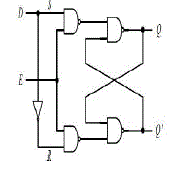
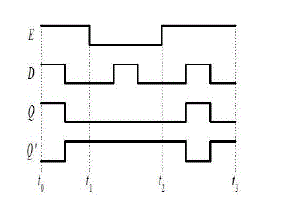
| This method replaces the BEC add one circuit by Dlatch
with enable signal. Latches are used to store one bit
information. Their outputs are constantly affected by their
inputs as long as the enable signal is asserted. In other words,
when they are enabled, their content changes immediately
according to their inputs. D-latch and it’s waveforms are shown
in Fig. 6 and Fig. 7 respectively [7]. |
| The architecture of proposed 16-b CSLA is shown in
Fig. 8. It has different five groups of different bit size RCA and
D-Latch. Instead of using two separate adders in the regular
CSLA, in this method only one adder is used to reduce the area,
power consumption and delay. Each of the two additions is
performed in one clock cycle. |
| This is 16-bit adder in which least significant bit
(LSB) adder is ripple carry adder, which is 2 bit wide. The
upper half of the adder i.e, most significant part is 14-bit wide
which works according to the clock. Whenever clock goes high
addition for carry input one is performed. When clock goes low
then carry input is assumed as zero and sum is stored in adder
itself. From the Fig. 9, it can understand that latch is used to
store the sum and carry for Cin=1. |
| Carry out from the previous stage i.e, least significant
bit adder is used as control signal for multiplexer to select final
output carry and sum of the 16-bit adder. If the actual carry
input is one, then computed sum and carry latch is accessed and
for carry input zero MSB adder is accessed. Cout is the output
carry. |
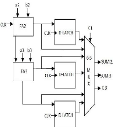
| The Fig.7 shows the internal structure of group 2 of
the proposed 16-bit CSLA. The group 2 performed the two bit
addition which are a2 with b2 and a3 with b3. This is done by
two full adder (FA) named FA2 and FA3 respectively. The
third input to the full adder FA2 is the clock instead of the carry
and the third input to the full adder FA3 is the carry output
from FA2. The group 2 structure has three D-Latches in which
two are used for store the sum2 and sum3 from FA2 and FA3
respectively and the last one is used to store carry. Multiplexer
is used for selecting the actual sum and carry according to the
carry is coming from the previous stage. The 6:3 multiplexer is
the combination of 2:1 multiplexer. |
| When the clock is low a2 and b2 are added with carry
is equal to zero. Because of low clock, the D-Latch is not
enabled. When the clock is high, the addition is performed with carry is equal to one. All the D-Latches are
enabled and store the sum and carry for carry is equal to one.
According to the value of c1 whether it is 0 or 1, the
multiplexer selected the actual sum and carry. |
| Fig. 9, 10 and 11 depicts that the newly proposed adder
consumes less area ,power and delay than the modified CSLA. |
CONCLUSION |
| A regular CSLA uses two copies of the carry
evaluation blocks, one with block carry input is zero and other
one with block carry input is one. Regular CSLA suffers from
the disadvantage of occupying more chip area. The modified
CSLA reduces the area and power when compared to regular
CSLA with increase in delay by the use of Binary to Excess-1
converter. This paper proposes a scheme which reduces the
delay, area and power than regular and modified CSLA by the
use of D-latches. Thus the ALU based test pattern generator
using this newly proposed carry select adder also consumes less
delay, area and power. |
Tables at a glance |
 |
 |
| Table 1 |
Table 2 |
|
Figures at a glance |
 |
 |
 |
 |
| Figure 1 |
Figure 2 |
Figure 3 |
Figure 4 |
 |
 |
 |
 |
| Figure 5 |
Figure 6 |
Figure 7 |
Figure 8 |
|
References |
- Antonis Paschalis, IoannisVoyiatzis, and DimitrisGizopoulos ,”Accumulator based 3 weight pattern generation,” IEEE Trans.Very Large Scale Integr. (VLSI) Syst., vol. 20, no. 2, pp. 357–361,Feb. 2012.
- E. Kalligeros, X. Kavousianos, D. Bakalis, and D. Nikolos, “Anefficient seeds selection method FOR LFSR-based test-per-clockBIST,” in Proc. Int. Symp. Quality Electron. Des. , 2002, p. 261.
- A. Stroele, “A self test approach using accumulators as test pattern generators,” in Proc. Int. Symp. Circuits Syst., 1995, pp.2120–2123.
- P. Hortensius, R. McLeod, W. Pries, M. Miller, and H. Card, “Cellular automata-based pseudorandom generators for built-inself test,” IEEE Trans. Comput.-Aided Des. Integr. Circuits Syst., vol. 8, no. 8, pp. 842–859, Aug. 1989.
- S. Wang, “Low hardware overhead scan based 3-weight weighted random BIST,” in Proc. IEEE Int. Test Conf., 2001, pp. 868–877.
- Voyiatzis, D. Gizopoulos, and A. Paschalis, “Accumulator-based weighted pattern generation,” presented at the IEEE Int. Line Test Symp., Saint Raphael, French Riviera, France, Jul. 2005.
- H.J. Wunderlich, “Self test using unequiprobable random patterns,” in Proc. 17th Int. Symp. Fault-Tolerant Comput.(FTCS), 1987, pp.258–263.
- B. Ramkumar and Harish M Kittur.” Low-Power and Area- Efficient Carry Select Adder,” IEEE Trans. Very Large ScaleIntegr. (VLSI) Syst., vol. 20, no. 2, pp. 371–375, Feb. 2012.
|