Keywords
|
| FFT; Carry Select Adder; Radix-2;VHDL |
INTRODUCTION
|
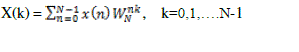
| To perform the frequency analysis on a discrete time signal, we convert the time domain sequence to an equivalent frequency domain representation. Such a representation is given by the Fourier transform.The discrete Fourier transform (DFT) is one of the Fourier transform, used for Fourier analysis. It transforms time domain signals to frequency domain signals [5]. In an N point DFT, to evaluate each DFT sample value, we have to perform N multiplications and N-1 additions using complex numbers. N such computations are required in all, therefore there will be N2 complex multiplications and N(N-1) complex additions. |
| The FFT procedure for synthesizing and analyzing the Fourier series was given by Cooley and Tukey.It is a computationally efficient way to calculate DFT. The wide usage of DFT’s in Digital Signal Processing applications is the motivation to implement FFT’s.This method provides a divide and conquer approach to the computation of DFT[2]. This is based on the decomposition of N point DFT into successively smaller DFTs[1]. In an N point sequence if N can be expressed as N = rm, then the sequence can be designated into r point sequences where m denotes the number of stages of computation and r denotes radix of the FFT algorithm. For example to perform radix 2 FFT algorithm, the value of N should be such that N = 2m. |
| Here the decimation can be performed ‘m’ times where m =log2N. The total number of complex additions are reduced to NlogrN and total number of complex multiplications are reduced to (N/2)logrN[1]. There are two methods of FFT: Decimation In Time (DIT), and Decimation In Frequency (DIF).In DIT, the inputs are fed in bit reverse order and the outputs are obtained in normal order. In DIF, the inputs are given in normal order to the butterfly unit and outputs are obtained in bit reversed format.This paper adopts Radix-2, decimation-in-time FFT algorithm[1]. |
RADIX-2 FFT ALGORITHM
|
| Radix-2 is the first FFT algorithm and was proposed by Cooley and Tukey in 1965[1]. The DFT of a given sequence x[n] can be computed using the formula |
 (1) (1) |
| where WN = e-j2π/N is the Twiddle factor which is referred to as roots of unity complex multiplicative constants in FFT computation[3]. They can be used to recursively combine smaller length DFTs. In radix-2 FFT, the N-point DFT can be decomposed into (N/2) point even and odd subsequences as [6]: |
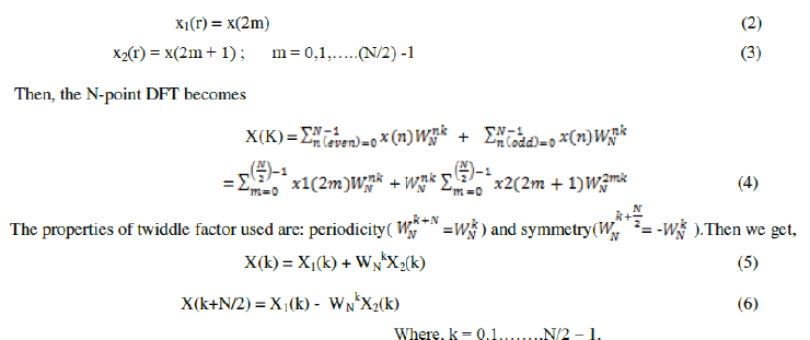 |
| If N is a regular power of 2, the same computational procedure can be applied recursively until the N-point DFT is evaluated as a collection of 2- point DFT's[5]. |
FFT ARCHITECTURE
|
| The block diagram of a general FFT architecture is shown in the figure 3. It consists of five basic blocks. A double port RAM memory to hold the values of input, output and intermediate operations, a Butterfly processing unit which consist of radix-2 butterflies and it is the heart of FFT algorithm, ROM memories to store twiddle factors and an address generation unit to extract data from RAM and ROM and finally a controller. |
| A. General Description |
| The whole FFT operation is partitioned into three processes: DATA LOAD, COMPUTATION AND RESULT UNLOAD. Initially input datas are given to the processor by means of siminputs. These datas are written into the RAM. The processing cycle starts with data load process. Here we read the stored data from RAM and start signal for FFT becomes high. Then, FFT computation of stored data takes place. Finally the results are stored in RAM and becomes available at the output[3]. |
| B. RAM |
| The RAM memory carries different types of data as the computation of FFT algorithm proceeds[3].Initially the input datas for FFT computation are stored in RAM. After each butterfly operations,it overwrites the input data positions. And finally during the output process bit reversed address is given to the RAM and it outputs the data accordingly. The dual port capability of RAM makes two data samples available at the sametime.So it decreases the overall computation time of FFT. |
| C. ROM |
| The ROM is used to store the sine and cosine values of twiddle factors needed in the FFT computation process[3]. It outputs these values according to the address given to it. |
| D. Butterfly Processing Unit |
| The butterfly is the basic operator of the FFT. It takes two data words from memory and computes the two point FFT. The input data are taken in 2’s complement format[3]. A butterfly unit consist of (N/2) butterflies and the basic structure is shown in the figure 4. Each unit contains two ROM memories to store sine and cosine co-efficients of twiddle factors, four 16x16 bit multipliers, six 32-bit accumulators and two concatenation operators to get the correct data format at the output. |
| The arithmetic operations involved in the butterfly unit is shown in the table I. The whole butterfly operation takes six instants of time. First, the two data inputs and the twiddle factor co-efficients are read(R).They are multiplied(x) to get the partial products in 16-bit format. Then, they are added and subtracted and truncated (+/-).The truncated real and imaginary parts are concatenated (&) to get the 32-bit format. |
| The adder used in butterfly computation is the carry select Adder (CSLA) which is one of the fastest adder [9]. The main advantage is that the arithmetic operations follows pipelining operation [4],[8] and addition is done using CSLA, so it reduces the overall computation time. |
| E. Address Generator |
| The purpose of address generation unit is to provide the ROM and RAM memory with correct address. It also keeps track of which butterfly is being computed in which stage. The block diagram of this unit is given in figure 5.For an 8- point complex FFT, there are 3 stages, each stage consisting of 4 butterflies. Since the address during input, output and FFT computation processes are different, it keeps track of the mode of operation of the chip and generates the required address [3]. Mode of operation information is supplied by the controller. |
| F. Controller |
| It controls the whole activity of FFT computation. It act as a combinational state logic. |
PROPOSED ADDER IN BUTTERFLY UNIT
|
| The adder circuit used in the butterfly structure is the carry select adder which consists of two Ripple Carry Adders (RCA) with C_in=0 and C_in=1 and a Multiplexer [9]. The problem in CSLA design is that it is not area efficient because it uses multiple pairs of RCA to generate partial sum and carry by considering carry input and then the final sum and carry are selected by the mux which is shown in the figure 6. |
| In order to improve the shortcomings of CSLA, we use Binary to Excess-1 Converter (BEC) instead of RCA with C_in =1 in the regular CSLA[9]. The structure of proposed adder is shown in the figure 7.The main advantage of this BEC logic comes from the lesser number of logic gates than the n-bit Full Adder(FA) structure. The modified CSLA architecture is therefore, having low area, low power, so it is simple and efficient for VLSI hardware implementation. |
RESULTS AND DISCUSSIONS
|
| After simulating both CSLA and proposed CSLA with BEC incorporated FFT, the design is synthesized using Xilinx ISE 8.1. A comparison between existing FFT and proposed FFT is done. |
| A. Comparison between CSLA and CSLA with BEC |
| Regular CSLA incorporated FFT is considered first. The device utilization summary of regular CSLA incorporated FFT is shown in the figure 8.Percentage of total number of Slice Registers and percentage of total number of 4 input LUTs is found to be 5% and 6% respectively. Also the total equivalent gate count for design is found to be a 10,898. |
| The device utilization summary of Modified CSLA with BEC incorporated FFT is shown in the figure 9. Percentage of total number of Slice Registers and percentage of total number of 4 input LUTs is found to be 4% and 5% respectively. |
| Also the total equivalent gate count for design is found to be a 9,789. |
| Table III shows the power consumption of both regular and modified CSLA incorporated FFT. The overall consumption of power is reduced from 334mW to 177mW in modified CSLA with BEC incorporated FFT. |
| Thus it is evident that resource utilization and power consumption is reduced in latter. So the CSLA with BEC in the design of butterfly unit optimize the area and power of FFT core. |
| B. Simulation result of 256-point FFT |
| The design is developed in VHDL language and simulated using ModelSim-Altera 6.4a. For the implementation of this circuit we have used Xilinx FPGA (XC4VLX15 device of Virtex 4). The top level source is Hardware Description Language type, with a XST (VHDL/VERILOG) environment.The simulated waveform of 256-point FFT is shown in figure 10. |
| The inputs of FFT are taken in 2’s complement format and the results are verified using MATLAB.The computation of FFT algorithm with different points can be simulated by varying the size of ROM and address generator unit while the size of other sub-blocks remains the same. This flexibility makes this FFT algorithm applicable for various re-configurable VLSI applications [7]. |
CONCLUSION
|
| The design of Radix-2 FFT with 256-point is done and simulated using Modelsim-Altera 6.4a Starter Edition. Our structure is synthesized in Xilinx ISE 8.1. A simple approach is proposed in this paper to reduce the area and power of FFT architecture. The reduced number of gates by replacing regular CSLA with modified CSLA with BEC offers the great advantage in the reduction of area and also the total power. |
Tables at a glance
|
|
|
Figures at a glance
|
 |
 |
 |
 |
 |
| Figure 1 |
Figure 2 |
Figure 3 |
Figure 4 |
Figure 5 |
 |
 |
 |
 |
 |
| Figure 6 |
Figure 7 |
Figure 8 |
Figure 9 |
Figure 10 |
|
References
|
- J. W. Cooley, J. W. Tukey, "An Algorithm for the Machine Calculation of Complex Fourier series," Math of comp, Vol. 19, pp.297-301, 1965
- Chu Chao, Zhang Qin, XieYingke, Han Chengde, ”Design of a High Performance FFT Processor Based on FPGA”, IEEE Proc.-Vis. ImageSignal Process, Vol. 152, No. 3, June 2005
- 3.C. González-Concejero, V. Rodellar,“ A portable hardware design of a FFT algorithm”, Latin American Applied Research,37:78-82, 2007
- Tze-Yun Sung, Hsi-Chin Hsin, “Reconfigurable VLSI Architecture for FFT Processor”, The International Arab Journal of InformationTechnology, Vol. 6, No. 1, January 2009
- SnehaN.kherde, MeghanaHasamnis, “Efficient Design and Implementation of FFT”, International Journal of Engineering Science andTechnology (IJEST), NCICT Special Issue February 2011
- Fangming Liu, Xiaozhong Pan,” Research on Implementation of FFT Based on FPGA”,2010 International Conference on Computer Applicationand System Modeling (ICCASM),Vol.7,pp.152-155,October 2010
- R.SaiBrunda, M.V.R. Vittal, “Design and Implementation of Variable Length FFT Processor for OFDMA System Using FPGA”, InternationalJournal of Engineering Research and Applications,Vol.3, Issue 2 , pp.1250-1253, March -April 2013
- A.A.Raut, S. M. Kate,” High Performance Pipelined Design for FFT Processor based on FPGA”, International Journal of Science and Research(IJSR), Volume 2 Issue 5, May 2013
- B. Ramkumar and Harish M Kittur,” Low-Power and Area-Efficient Carry Select Adder”, IEEE Transactions on Very Large Scale Integration(VLSI) Systems, Vol. 20, No. 2, February 2012
|