Keywords
|
| DC-DC converter, Continuous Conduction Mode, Discontinuous Conduction Mode, Grid system |
INTRODUCTION
|
| Generally, electric power generated by renewable energy sources is unstable in nature, thus producing a bad effect on the utility grid. This fact spurs research on energy storage systems to smooth out active-power flow on the utility grid. Simplified existing energy storage system employing a line-frequency (50- or 60-Hz) transformer, a PWM converter, a bidirectional chopper, and an energy storage device such as electric double layer capacitors (EDLCs) or lithium-ion batteries[1]. The transformer is indispensable for some applications that require voltage matching and/or galvanic isolation between the utility grid and the energy storage device. Replacing the line-frequency transformer with a high-frequency isolated dc-dc converter would make the energy storage system more compact and flexible[2]. Various bidirectional isolated dc-dc converters have been proposed as the interface to energy storage devices with focus on automotive or fuel cell applications. Most of the presented dc-dc converters have asymmetrical circuit configurations to couple the two dc links having largely different voltages, several tens volts and several hundred volts. |
| A bidirectional isolated dc-dc converter presented in 1991. It had two symmetrical single-phase voltage-source full-bridge converters. It suffered from a low efficiency because the first-generation IGBTs were used as switching power devices at that time. However, advancement in power device technology over the last decade has enabled the dcdc converter to operate at an efficiency as high as 97% by using the latest trench-gate IGBTs. A similar dc-dc converter has also achieved an efficiency of 97%. In addition, the use of silicon-carbide power devices in the near future will raise it to 99%[3]. Therefore, the dc-dc converter has become a promising candidate as a power electronic interface for an energy storage system. A bidirectional converter has been discussed to exchange electric power between a fuel cell, a battery, and a load, based on a three-port extension of the circuit presented[4]. The energy storage system using the bidirectional isolated dc-dc converter appropriately choosing the transformer turn ratio enables to design the voltage rating of the energy storage device, independent of the utility voltage[5]. The energy storage device is directly connected to one of the dc links of the dc-dc converter without any chopper circuit. Nevertheless, the dc-dc converter continues operating even when the voltage across the energy storage device, Vd2drops along with its discharge. Here Vd1 is input side DC voltage and Vd2 is DC output secondary voltage |
CIRCUIT CONFIGURATION
|
| The power conversion circuit of the proposed hybrid-input dc-to-dc converter is shown in Fig. 1, [4]-[8]which is essentially an integration of a boost converter and a buck-boost converter. The integrated power converter consists of two active power switches, S1 and S2, for boost conversion and buck-boost conversion, respectively, by commonly using a diode, D, an inductor, L, and a filter capacitor, C. The two dc sources, Vin1 and Vin2, are treated as the primary and secondary sources, depending on the capacity and the dependability of the power sources. The primary source has a capability of providing more energy to the load and is more durable than the secondary source is[9]. Two active power switches are turned on and off periodically at a same frequency but are activated alternately in a period. The powers delivered by two sources are coordinated by controlling their duty-ratios |
CIRCUIT OPERATION
|
| The power conversion circuit can be operated at the continuous conduction mode (CCM) or the discontinuous conduction mode (DCM), depending on the continuity of the inductor current. According to the status of three power switches, S1, S2, and D, this circuit operation can be divided into four stages, as shown in Fig. 2. [10]In which, the dutyratios of two active power switches are d1 and d2, respectively. At the CCM, the power conversion circuit is operated through Stages I, II, and III sequentially in a switching period, TS . Stage IV occurs only at the DCM when the inductor current falls down to zero. The steady state operation is described in the followings |
| Stage1 [t1-t2]: As the active power switch S2 is turned on, the diode D will be reversely biased and turned off. The inductor is charged by the secondary voltage source, V2, and the inductor current, iL, increases linearly |
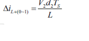 (1) (1) |
| In this stage, the filter capacitor delivers the stored energy to the load. |
| Stage II [t1~t2]: As S2 is turned off, the active power switch, S1 is turned on, and the diode D is now still turned off. The primary dc power source is providing electromotive force for charging the inductor in this stage. At the same time, iL increases linearly after preceding stage |
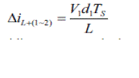 (2) (2) |
| The filter capacitor is still providing energy to the load in this stage. |
| Stage III [t2~t3]: When the power switch S1 is turned off, the diode D is forced to be turned on to conduct the inductor current. In this stage, the load draws energy from the primary source and the inductor |
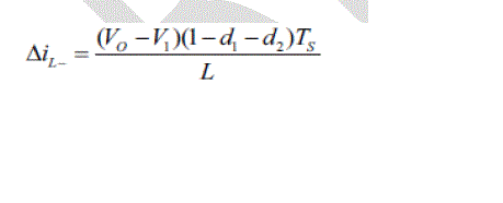 (3) (3) |
| Stage IV [t3~t4]: This stage only happened when the inductor current declines to zero, both S and D are turned off. The filter capacitor supplies a current to the load, and voltage on the capacitor declines. Fig. 3 depicts the theoretical waveforms on the key components of the power converter for CCM and DCM operations, respectively |
A. Continuous Conduction Mode
|
| The relationship between the two input voltages, V1 and V2, and the output voltage, Vo, can be obtained by the voltage-second balance. The output voltage of the power converter is the sum of V1 and the buck-boost conversion output voltage from V1 and V 2. This equation indicates the output voltage is always higher than the input voltage. In practice, the sum of d1 and d2 in one cycle is limited to be less than 0.9. |
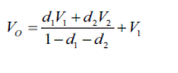 (4) (4) |
| Theoretically, the output power is the sum from two inputs In (5), I1 ' is the input current of the primary source at stage II while I1 is the sum of I1 ' and the output current IO. |
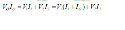 (5) (5) |
| In (5), I1 ' is the input current of the primary source at stage II while I1 is the sum of I1 ' and the output current IO. |
 (6) (6) |
| Then, the output current can be obtained as |
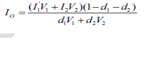 (7) (7) |
| Fig. 4 shows the relationship between the voltage step-up ratio with respect to the duty-ratios of the two active power switches under different input voltages. In which, the ratio between d1 and d2 is denoted by α |
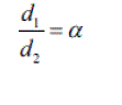 (8) (8) |
| And, the ratio between the two input voltages is denoted byβ It is noted that d2 is the dominant parameter that affects the variation of the output voltage rather than d1. In the figure, there d1 curve represents the characteristic of boost conversion when V2 is zero. |
B.Discontinuous Conduction Mode
|
| With a smaller inductance, the inductor current may decrease to zero when both active power switches have been turned off. |
| The boundary inductance can be calculated as |
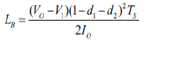 (10) (10) |
| By substituting (4) into (10), the boundary inductance can be rewritten as |
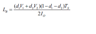 (11) (11) |
| The duty-ratio for decreasing the inductor current is denoted by d3. Then, the relationship between the two input voltage and the output voltage can be obtained as |
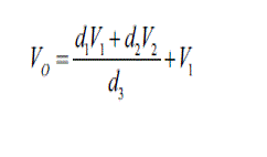 (12) (12) |
| The output current of the converter is |
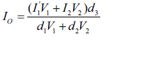 (13) (13) |
SIMULATION RESULTS
|
| A. Continuous Conduction Mode and Discontinuous Conduction Mode |
| B. Continuous Conduction Mode and Discontinuous Conduction Mode by using Grid connected |
CONCLUSION
|
| This paper proposed a three-port grid based dc-to-dc power conversion circuit which can be powered from two sources. The power coordination between two sources and the voltage regulation can be made by adjusting the duty-ratios of two active power switches and gate triggering pulses. As compared with the conventional multiple-input power converter, the proposed conversion circuit has less component count. The power conversion circuit can be used in a low range distributed system with two different ac and dc type power source |
Figures at a glance
|
 |
 |
 |
 |
| Figure 1 |
Figure 2 |
Figure 3 |
Figure 4 |
 |
 |
 |
 |
| Figure 5 |
Figure 6 |
Figure 7 |
Figure 8 |
 |
 |
 |
 |
| Figure 9 |
Figure 10 |
Figure 11 |
Figure 12 |
 |
 |
 |
 |
| Figure 13 |
Figure 14 |
Figure 15 |
Figure 16 |
|
References
|
- P. F. Ribeiro, B. K. Johnson, M. L. Crow, A. Arsoy, and Y. Liu, “Energy storage systems for advanced power applications,,” Proc. IEEE, vol. 89 , no. 12, pp. 1744–1756, Dec. 2001.
- T. Kinjo, T. Senjyu, N. Urasaki, and H. Fujita, “Output levelling of renewable energy by electric double layer capacitor applied for energy storage system,” IEEE Trans. Energy Convers., vol. 21, no. 1, pp. 221–227, Mar. 2006.
- M. Jain, M. Daniele, and P. K. Jain, “A bidirectional dc-dc converter topology for lowpower application,” IEEE Trans. Power Electron., vol. 15, no. 4, pp. 595–606, Jul. 2000.
- T. Kohama, M. Yamashima, and T. Nishimiya, “Operation-mode control of active-clamped bi-directional flyback converter as EDLC charger and discharger,” in Proc. Power Conversion Conf. (PCC), Osaka, Japan, 2002, vol. 3, pp. 1155–1159.
- A. D. Swingler and W. G. Dunford, “Development of a bi-directional dc/dc converter for inverter/charger applications with consideration paid to large signal operation and quasi-linear digital control,” in Proc. IEEE Power Electronics Specialists Conf. (PESC), 2002, vol. 2, pp961–966.
- F. Z. Peng, H. Li, G.-J. Su, and J. S. Lawler, “A new ZVS bi-directional dc-dc converter for fuel cell and battery application,” IEEE Trans. Power Electron., vol. 19, no. 1, pp. 54–65, Jan. 2004.
- L. Zhu, “A novel soft-commutating isolated boost full-bridge ZVS-PWM dc-dc converter for bi-directional high power applications,” IEEE Trans. Power Electron., vol. 21, no. 2, pp. 422–429, Mar. 2006.
- L. Shi, L. Sun, D. Xu, and M. Chen, “Optimal design and control of 5 kWPWMplus phase-shift (PPS) control bidirectional dc-dc converter,” in Proc. IEEE Appl. Power Electron. Conf. Expo (APEC), Dallas, TX, Mar. 2006.
- Y. Hu, J. Tatler, and Z. Chen, “A bi-directional dc/dc power electronic converter for an energy storage device in an autonomous power system,” in Proc. Power Electron. Motion Cont. Conf. (IPEMC), 2004, vol. 1, pp. 171–176.
- H.-J. Chiu and L.-W. Lin, “A bidirectional dc-dc converter for fuel cell electric vehicle driving system,” IEEE Trans. Power Electron., vol. 21, no. 4, pp. 950–958, Jul. 2006.
|