Keywords
|
| High Step-up Converter, Voltage Multiplier module, Boost Converter, photovoltaic system |
INTRODUCTION
|
| Renewable sources of energy are increasingly valued worldwide because of energy shortage and environmental contamination. Renewable energy systems generate low voltage output; thus, high step-up dc/dc converters are widely employed in many renewable energy applications, including fuel cells, wind power, and photovoltaic systems . Among renewable energy systems, photovoltaic systems are expected to play an important role in future energy production . Such systems transform light energy into electrical energy, and convert low voltage into high voltage via a step-up converter, which can convert energy into electricity using a grid-by-grid inverter or store energy into a battery set. Fig. 1 shows a typical photovoltaic system that consists of a solar module, a high step up converter, a charge-discharge controller, a battery set, and an inverter. |
| The high step-up converter performs importantly among the system because the system requires a sufficiently high step-up conversion. Theoretically, conventional step-up converters, such as the boost converter and fly back converter, cannot achieve a high step-up conversion with high efficiency because of the resistances of elements or leakage inductance. Thus, a modified boost–fly back converter was proposed, and many converters that use the coupled inductor for a considerably high voltage conversion ratio were also proposed. |
LITERATURE SURVEY
|
| Conventional step-up converters, such as the boost converter and fly back converter, cannot achieve a high step-up conversion with high efficiency because of the resistances of elements or leakage inductance .Conventional step-up converters with a single switch are unsuitable for high-power applications given an input large current ripple, which increases conduction losses. |
| Thus, numerous interleaved structures and some asymmetrical interleaved structures are extensively used . The current study also presents an asymmetrical interleaved converter for a high step-up and high-power application. Modifying a boost–fly back Converter. One of the simple approaches to achieving high step-up gain; this gain is realized via a coupled inductor. The performance of the converter is similar to an active-clamped fly back converter; thus, the leakage energy is recovered to the output terminal. |
PROPOSED SYSTEM
|
| It obtains extra voltage gain through the voltage-lift capacitor, and reduces the input current ripple, which is suitable for power factor correction (PFC) and high-power applications. In this paper, an asymmetrical interleaved high step-up converter that combines the advantages of the aforementioned converters is proposed, which combined the advantages of both. In the voltage multiplier module of the proposed converter, the turns ratio of coupled inductors can be designed to extend voltage gain, and a voltage-lift capacitor offers an extra voltage conversion ratio. |
| The advantages of the proposed converter are as follows: |
| 1) the converter is characterized by a low input current ripple 0and low conduction losses, making it suitable for high power applications; |
| 2) The converter achieves the high step-up voltage gain that renewable energy systems require; |
| 3) Leakage energy is recycled and sent to the output terminal, and alleviates large voltage spikes on the main switch; |
| 4) The main switch voltage stress of the converter is substantially lower than that of the output voltage; |
| 5) Low cost and high efficiency are achieved by the low rDS(on) and low voltage rating of the power switching device. |
A) OPERATING PRINCIPLE DESCRIPTION:
|
| The proposed high step-up converter with voltage multiplier module is shown in Fig. 3(a). A conventional boost converter and two coupled inductors are located in the voltage multiplier module, which is stacked on a boost converter to form an asymmetrical interleaved structure. Primary windings of the coupled inductors with Np turns are employed to decrease input current ripple, and secondary windings of the coupled inductors with Ns turns are connected in series to extend voltage gain. The turns ratios of the coupled inductors are the same. The coupling references of the inductors are denoted by “.” and “*” in Fig. 3. |
| The equivalent circuit of the proposed converter is shown in Fig. 3(b), where Lm1 and Lm2 are the magnetizing inductors, Lk1 and Lk2 represent the leakage inductors, S1 and S2 denote the power switches, Cb is the voltage-lift capacitor, and n is defined as a turns ratio Ns /Np. |
| The proposed converter operates in continuous conduction mode (CCM), and the duty cycles of the power switches during steady operation are inter leaved with a 180? phase shift; the duty cycles are greater than 0.5. The key steady waveforms in one switching period of the proposed converter contain six modes, which are depicted in Fig shows the topological stages of the circuit. |
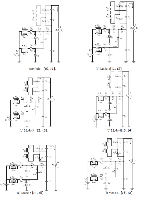 |
| Mode 1 [t0, t1]: At t=t0, the power switches S1 and S2 are both turned ON. All of the diodes are reversed-biased. Magnetizing inductors Lm1 and Lm2 as well as leakage inductors Lk1 and Lk2 are linearly charged by the input voltage source Vin. |
| Mode 2 [t1, t2]: At t=t1, the power switch S2 is switched OFF, thereby turning ON diodes D2 and D4. The energy that magnetizing inductor Lm2 has stored is transferred to the secondary side charging the output filter capacitor C3. The input voltage source, magnetizing inductor Lm2, leakage inductor Lk2, and voltage-lift capacitor Cb release energy to the output filter capacitor C1 via diode D2, there by extending the voltage on C1. |
| Mode 3 [t2, t3]: At t=t2, diode D2 automatically switches OFF because the total energy of leakage inductor Lk2 has been completely released to the output filter capacitor C1. Magnetizing inductorLm2 transfers energy to the secondary side charging the output filter capacitor C3 via diode D4 until t3. |
| Mode 4 [t3, t4]: At t=t3, the power switch S2 is switched ON and all the diodes are turned OFF. The operating states of modes 1 and 4 are similar. |
| Mode 5 [t4, t5]: At t=t4, the power switch S1 is switched OFF, which turns ON diodes D1 and D3. The energy stored in magnetizing inductor Lm1 is transferred to the secondary side charging the output filter capacitor C2. The input voltage source and magnetizing inductor Lm1 release energy to voltage-lift capacitor Cb via diode D1, which stores extra energy in Cb. |
| Mode 6 [t5, t0]: At t=t5, diode D1 is automatically turned OFF because the total energy of leakage inductor Lk1 has been completely released to voltage-lift capacitor Cb. Magnetizing inductor Lm1 transfers energy to the secondary side charging the output filter capacitor C2 via diode D3 until t0. |
CONVERTER COMPONENTS AND PARAMETERS
|
 |
| The high step-up interleaved converter introduced in is also suitable as a candidate for high step-up, high-power conversion of the PV system, and the other high step-up interleaved converter introduced in , which is an asymmetrical interleaved structure as proposed converter is favourable for dc-micro grid applications. Both of converters use coupled inductor and voltage double to achieve high step-up conversion. For the proposed converter, the step-up gain is highest and the voltage stress on switch is the lowest, as converter introduced. Under the turns ratio n designed as less than 2, the highest voltage stress on diodes of the proposed converter is the lowest among the compared converters. In addition, the quantities of diodes are the least as converter introduced .Because the components of the proposed converter are the least among the compared converters, the reliability is higher and the cost is lower. Thus, the proposed converter is suitable for high step-up, high-power applications such as PV system. In control strategy, the proposed converter is controlled by the microchip dsPIC30F4011 as shown in Fig. 5 PV module and battery set are the main input power sources, which can be seen as an equivalent voltage source for the proposed converter, and the MPPT algorithm is employed by referring . The battery management system (BMS) for the charge/discharge controller is not the main priority in this paper; thus, the related designed is not implemented in the paper. |
DESIGN AND EXPERIMENTAL RESULTS
|
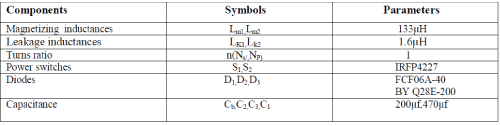
| A prototype of the proposed high step-up converter with a40-V input voltage, 380-V output voltage, and maximum output power of 1 kW is tested. The switching frequency is 40 kHz, and the corresponding component parameters are listed in Table II for reference .The design consideration of the proposed converter includes component selection and coupled inductors design, which are based on the analysis presented in the previous section. In the proposed converter, the values of the primary leakage inductors of the coupled inductors are set as close as possible for current sharing performance. Due to the performances of high step-up gain, the turns ratio n can be set 1 for the prototype circuit with a 40- V input voltage, 380- V output to reduce cost, volume, and conduction loss of winding. Thus, the copper resistances which affect efficiency much can be decreased. |
| Fig.6(a) illustrates the measured waveforms of Vgs1, Vgs2,, iLK1, iLK2, Vds1, Vds2 and ils at Po = 1 kW. In Fig. 6, the switch voltage is clamped at 90 V, which is much smaller than the output voltage 380 V. Fig. 6(b) illustrate the Measured waveforms of Vgs1, Vgs2, iD1, iD2, iD3 ,and iD4 at Po = 1 kW. The measured waveforms are consistent with the steady-state analysis. |
| Fig. 6(b) illustrate the Measured waveforms of Vgs1, Vgs2, iD1, iD2, iD3 ,and iD4 at Po = 1 kW. The measured waveforms are consistent with the steady-state analysis. |
| Fig. 7 shows the simulation and experimental result of voltage on all capacitor to illustrate the high voltage storage and theoretical analysis. Vc1 is equal to Vcb plus output voltage of boost converter, and Vcb is equal to the output voltage of the boost converter. Thus, Vc1 is twice of Vcb. Vc2 is equal to Vc3 ;both are nearly Vcb because turns ratio n is set 1. |
| Fig.8 shows the input current ripple iin and the currentsiLK1 and iLK2 the primary side of the coupled inductors at Po = 1 kW. The peak-to-peak current ripple is about 2 A (6%) ,which confirms that the input current ripple is very low even if at high-power operation. |
| Figure 9: shows the measured efficiency of the proposed converter. The maximum efficiency is 96.8% at Po = 400 W. At maximum output power, the conversion efficiency is about 96.1%. |
CONCLUSION
|
| This paper has presented the topological principles, steady state analysis, and experimental results for a proposed converter. The proposed converter has been successfully implemented in an efficiently high step-up conversion without an extreme duty ratio and a number of turns ratios through the voltage multiplier module and voltage clamp feature. The interleaved PWM scheme reduces the currents that pass through each power switch and constrained the input current ripple by approximately 6%. The experimental results indicate that leakage energy is recycled through capacitor Cb to the output terminal. Meanwhile, the voltage stresses over the power switches are restricted and are much lower than the output voltage (380 V). These switches, conducted to low voltage rated and low on-state resistance MOSFET, can be selected. Furthermore, the full-load efficiency is 96.1% at Po = 1000 W, and the highest efficiency is 96.8% at Po = 400 W. Thus, the proposed converter is suitable for PV systems or other renewable energy applications that need high step-up high-power energy conversion. |
Figures at a glance
|
 |
 |
 |
 |
 |
| Figure 1 |
Figure 2 |
Figure 3 |
Figure 4 |
Figure 5 |
 |
 |
 |
 |
 |
| Figure 6 |
Figure 7 |
Figure 8 |
Figure 9 |
Figure 10 |
|
| |
References
|
- C. Hua, J. Lin, and C. Shen, “Implementation of a DSP-controlled photovoltaic system with peak power tracking,” IEEE Trans. Ind. Electron.,vol. 45, no. 1, pp. 99–107, Feb. 1998.
- J. M. Carrasco, L. G. Franquelo, J. T. Bialasiewicz, E. Galvan, R. C. P. Guisado, M. A. M Prats, J. I. Leon, and N. Moreno-Alfonso, “Powerelectronic systems for the grid integration of renewable energy sources: A survey,” IEEE Trans. Ind. Electron., vol. 53, no. 4, pp. 1002– 1016, Jun. 2006.
- J. T. Bialasiewicz, “Renewable energy systems with photovoltaic power generators: Operation and modeling,” IEEE Trans. Ind. Electron., vol. 55, no. 7, pp. 2752–2758, Jul. 2008.
- Y. Xiong, X. Cheng, Z. J. Shen, C. Mi, H.Wu, and V. K. Garg, “Prognostic and warning system for power-electronic modules in electric, hybrid electric, and fuel-cell vehicles,” IEEE Trans. Ind. Electron., vol. 55, no. 6, pp. 2268–2276, Jun. 2008.
- F. S. Pai, “An improved utility interface for micro-turbine generation system with stand-alone operation capabilities,” IEEE Trans. Ind. Electron., vol. 53, no. 5, pp. 1529–1537, Oct. 2006.
- H. Tao, J. L. Duarte, and M. A. M. Hendrix, “Line-interactive UPS using a fuel cell as the primary source,” IEEE Trans. Ind. Electron., vol. 55, no. 8, pp. 3012–3021, Aug. 2008.
- Z. Jiang and R. A. Dougal, “A compact digitally controlled fuel cell/battery hybrid power source,” IEEE Trans. Ind. Electron., vol. 53, no. 4, pp. 1094–1104, Jun. 2006.
|