Keywords
|
| Boost converter, Coupled Inductor, Diode Capacitor, Voltage Multiplier cell, voltage stress |
INTRODUCTION
|
| Now a day, single switch high voltage gain dc –dc converters is used to reduce voltage stress and recycle the output by leakage inductance energy. In this converter used in many industrial applications such as fuel cell energy conversion systems, uninterrupted power supply electric traction and some medical equipment’s. The above applications depend on the dc- dc converter types which are boost converter. Here with the help of boost converter rather than classical, high output voltage is equal to voltage stress of the main switch. The result of an extremely high duty cycle will give large conduction losses on power device and it is not realizing high voltage gain. This converter achieve high conversion ratio and reduced at extremely high duty cycle. In high voltage applications the rating of active switch is high voltage must be selected. |
| The converters based on transformers or coupled inductors or tapped inductors used to achieve the high conversion ratio of voltage [5]–[6]. The quadratic boost converter using a single active switch is another interesting topology for extending the voltage gain [1]–[3], the turn ratio of the coupled inductor or tapped inductor is increased. For improving the voltage conversion ratio, the input current ripple becomes larger [8]–[9].the digital based system has implemented for controlling the output [12]. |
| A single switch high voltage dc-dc converter consist of switched capacitor, switched inductor ,clamper circuit and voltage doublers with capacitor and diode and these are the components used to reduced voltage stress and obtain reliable voltage high output. To attain the conversion ratio in high level, the transformer can be used without operating it in duty cycle in higher level. The filter circuit is used to the unwanted ripples. With the help of duty cycle, the level of output voltage can be estimated and moderate voltage gain is found. Advantages of a single switch high voltage gain converter with coupled inductor and diode capacitor method: (1)To eliminate potential resonance between leakage inductor and diode capacitor.(2)Coupled inductor used to increased efficiency of voltage gain and recycle leakage inductor energy. The existing system, proposed system, simulation results using MATLAB has been discussed in the following sections. |
EXISTING CONVERTER
|
| The dc power supply is used many industries and domestics applications. The nonlinear load produces abnormal conditions such as voltage imbalance, sudden fluctuation, high ripple current and harmonics current. During these conditions the power factor will be low. Mostly power electronics applications are used rectifiers, that converter is convert DC to AC in a switch mode and conventional mode types, these contribute the high total harmonics distortion ,low power factor and low efficiency in the power system. Due to the harmonics current, voltage distortion and reduced supply energy capacity at lines, these are caused in the power system. So these problems reduced by using a single switch high voltage gain converter that is consist on clamped circuit, voltage doubler cell and capacitor filters are used. Then coupled inductor is used to reduce the ripple current in the converter. Thus the proposed converter is to reduced voltage stress and it is able to give high voltage gain. This converter is used to improve the high conversion ratio |
COUPLED INDUCTOR, CLAMPED CIRCUIT AND VOLTAGE DOUBLER CELL
|
| The proposed converter is consisting on coupled inductor or transformers, clamped circuit, voltage multiplier cell and diode capacitors. The coupled inductors have been used to achieve high voltage conversion ratio without operating extremely high duty ratio and high voltage gain. Then the clamped is an electronic circuit that prevents signal from exceeding a certain defined magnitude by shifting its dc value and it does not restrict the peak to peak excursion of the signal, but move it up and down by a fixed value. With the help of diode which conducts electric current in only one direction, then resistor and capacitor in the circuit are used to maintain an altered dc level at the clamper output. Then the voltage doublers cell is also electronic circuit which charges capacitors from the input voltage and switches these charges in such a way that, in the ideal case , exactly twice the voltage is produced at the output as its input. So using above elements to achieve high voltage gain, low voltage stress and recycle the output energy by using leakage inductance |
PROPOSED CONVERTER
|
| The boost converter not able to provide high voltage gain ,so designed high efficiency of A single switch high voltage gain dc dc converter with coupled inductor and diode capacitor methods.The proposed converters of this project are to reduce the voltage stress and obtain high voltage gain by using the high voltage gain dc to dc converters. Therefore the active switch of voltage stress is reduced and improves the conversion efficiency. A high voltage gain dc-dc converters is consist on given parameters |
| Q=MOSFET switch |
| N1, N2= coupled inductors |
| Li=input inductor |
| Vin= input voltage |
| D1,D2, and D3 =diodes |
| C1,C2, and C3=capacitors |
| D0, = output diode |
| Dr= regeneration diode |
| C0=output capacitor |
| V0=output voltage and |
| R = resistive load |
| The above mentioned parameters are shown in MATLAB diagram and we made the following assumptions to analysis the circuits |
| • All components are ideal except coupled inductor |
| • The voltage across the each capacitor is considered to beconstant. |
| • Coupled inductors act as continuous conduction and discontinuous conduction mode.These are assumptions presents in the high voltage gain converters. The fig.1 block diagram of high voltage gain converter consist of dc supply clamper circuit,voltage doubler cell, PI controller and load. |
CIRCUIT ANALYSIS OF CONDUCTION MODES PROCESS
|
| A single switch high voltage gain converter with coupled inductor and diode capacitor is containing two modes of conduction process such as continuous conduction mode and discontinuous conduction mode. These modes are discussed by using stage time period and devices ON and OFF period. With help of PI controller reduced the error output. The circuit diagram of high voltage gain converter with coupled inductor and capacitor has been shown in the fig.2 |
SIMULATION RESULT AND ANALYSIS
|
| The operations of the proposed converter have been given in the table 1 & 2 in the form of continuous and discontinuous mode. The simulation circuit is used to verify the performance of output. The input voltage is 18-36V and to obtain the output voltage is 380V. |
Simulation parameter for the given circuit Fig(4) has been given below
|
| Input voltage =18-36V |
| Capacitor(C1,C2,C3,C0) =1μF,220μF |
| Frequency = 40 KHZ |
| Input inductor= 40μF |
| Output voltage= 380V |
| The duty cycle ration and inductance value has been calculated using the below formula |
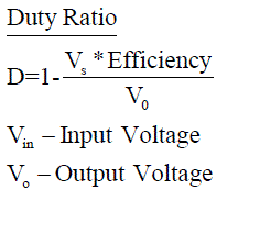 (1) (1) |
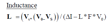 (2) (2) |
| From the purposed converter, input voltage is 25.1V and obtained the ripple free voltage of 375V shown in the waveform Fig.5. The reduced voltage distortion with high voltage gain is obtained in the proposed converter |
CONCLUSION
|
| The proposed converter is used to reduce voltage distortion and using integrated coupled inductor to reduce voltage stress. To obtain high voltage gain by using high voltage gain converter with coupled inductor and diode capacitor and this converter mostly used in industrial applications. To achieve high conversion ratio depends on without high duty cycle. The proposed converter is reliable and cost of it is low and also leakage inductance of coupled inductor is used to recycle the energy efficiently |
ACKNOWLEDGEMENT
|
| The authors are would like to thank to theManagement Trustees of IFET College of Engineering, Prof.Dr.G.Mahendran,Principal, IFET College of Engineering, Prof.S.MatildaDean Academics, Prof.R.Malar HoD/EEE,IFET College of Engineeringfor providing necessary facilities for the preparation of paper |
Tables at a glance
|
 |
|
| Table 1 |
Table 2 |
|
| |
Figures at a glance
|
 |
 |
 |
 |
 |
| Figure 1 |
Figure 2 |
Figure 3 |
Figure 4 |
Figure 5 |
|
| |
References
|
- L. H. Barreto, E. A. Coelho, V. J. Farias, J. C. de Oliveira, L. C. de Freitas,and J. B.Vieira, “A quasi-resonant quadratic boost converter using a singleresonant network,” IEEE Trans. Ind. Electron., vol. 52, no. 2, pp. 552–557,Apr. 2005.
- E. H. Ismail, M. A. Al-Saffar, A. J. Sabzali, and A. A. Fardoun, “Highvoltage gain single-switch non-isolated DC-DC converters for renewableenergy applications,” in Proc. IEEE Int. Conf. Sustainable Energy Technol.Conf., Dec. 2010, pp. 1–6.
- L. H. S. C. Barreto, E. A. A. Coelho, L. C. Freitas, V. J. Farias, andJ. B. Vieira, Jr., “An optimal lossless commutation quadratic PWM boostconverter,” in Proc. IEEE App. Power Electron. Conf. Expo., Dallas, TX,USA, 2002, vol. 2, pp. 624–629.
- K. D. Kim, J. G. Kim, Y. C. Jung, and C. Y.Won, “Improved non-isolatedhigh voltage gain boost converter using coupled inductors,” in Proc. IEEEInt. Conf. Electric. Mach. Syst., Aug. 2011, pp. 20–23.
- G. Spiazzi, P. Mattavelli, J. R. Gazoli, R. Magalhaes, and G. Frattini,“Improved integrated boost-flyback high step-up converter,” in Proc. IEEEInd. Technol. Conf., Mar. 2010, pp. 1169–1174.
- K. B. Park,G. W.Moon, andM. J.Youn, “Non-isolated high step-up boostconverter integratedwith SEPIC converter,” IEEE Trans. Power Electron.,vol. 25, no. 9, pp. 1791–1801, Sep. 2010.
- N. Vazquez and L. Estrada, “The tapped-inductor boost converter,” inProc. IEEE Int. Symp. Ind. Electron., Jun. 2007, pp. 531–538.
- T.-F. Wu, Y.-S.Lai, J.-C.Hung, and Y.-M. Chen, “Boost converter withcoupled inductors and buck-boost type of active clamp,” IEEE Trans. Ind.Electron., vol. 55, no. 1, pp. 154–162, Jan. 2008.
- T. J. Liang and K. C. Tseng, “Analysis of integrated boost-flyback step upconverter,” IEE Proc. Electron. Power Appl., vol. 152, no. 2, pp. 217–225,Mar. 2005.
- W. Li and X. He, “A family of interleaved DC–DC converters deducedfrom a basic cell wnding-cross-coupled inductors (WCCIs) for high stepup or step-down converters,” IEEE Trans. Power Electron., vol. 23, no. 4,pp. 1791–1801, Jul. 2008.
- Y. Deng, Q. Rong, W. Li, Y. Zhao, J. J Shi, and X. N.He, “Single-switchhigh step-up converters with built-in transformer voltage multiplier cell,”IEEE Trans. Power Electron., vol. 27, no. 8, pp. 3557–3567, Aug. 2012.
- J.Baskaran, P.Pugazhendiran, M.Sujith, “A novel Digitally Controlled Converter for Renewable Energy Resources” , International Journal of Innovative Technology and Exploring Engineering (IJITEE) ,Volume-2, Issue-4, March 2013
|