Keywords
|
| Nine Switch, UPQC, Non Linear Load, and PWM Control. |
INTRODUCTION
|
| Nowadays, modern industrial devices are mostly based on electronic devices such as programmable logic controllers and electronic drives. The electronic devices are very sensitive to disturbances and become less tolerant to power quality problems such as voltage sags, swells and harmonics. Voltage dips are considered to be one of the most severe disturbances to the industrial equipment’s. Voltage support at a load can be achieved by reactive power injection at the load point of common coupling. The common method for this is to install mechanically switched shunt capacitors in the primary terminal of the distribution transformer. The mechanical switching may be on a schedule, via signals from a supervisory control and data acquisition (SCADA) system, with some timing schedule, or with no switching at all. The disadvantage is that, high speed transients cannot be compensated. Some sag is not corrected within the limited time frame of mechanical switching devices. Transformer taps may be used, but tap changing under load is costly. Where the nine-switch converter is chosen to replace a shunt and a series converter found in an integrated power conditioner, instead of two shunt converters. Underlying operating principles are discussed comprehensively to demonstrate how such “series– shunt” replacement can bring forth the full advantages of the nine-switch converter, while yet avoiding those limitations faced by existing applications. Details explaining smooth transitions between normal and sag operating modes are also provided to clarify that the more restricted nine-switch converter will not underperform the more independent back-to-back converter even for sag mitigation. |
| Then proceeds to compare the ratings and losses of the back-to-back and nine-switch conditioners, before an appropriate modulation scheme is evaluated in reducing the nine-switch converter commutation count, and hence it’s switching losses. Also presented in two sets of higher level control schemes with the first used for controlling one set of three-phase outputs so as to compensate for harmonic currents reactive power flow and three-phase unbalance caused by nonlinear loads. |
PROPOSED SYSTEM
|
EXISTING SYSTEM
|
| In Existing method 12 switches were used and switching losses are high in this method. Total harmonic distortions are high in this shown fig 5.1. When applied to the nine-switch converter, then lead to those output voltage transitional for representing V per phase. Together, these voltage transitions show that the forbidden state and is effectively blocked off. The blocking is, how-ever, attained at the incurrence of additional constraints limiting the reference amplitudes and phase shift. These limitations are especially prominent for references having sizable amplitudes and/or different frequencies, as exemplified by the illustrative cases. The two references of different frequencies limited to a maximum modulation ratio of 0.5 each, extendible by 1.15 times if triplen offset is added, in order to avoid crossover. The limited phase-shift constraint, associated with references of the same frequency and combined modulation ratio of greater than 1.15 with triplen offset added which indeed is a neat and intelligent application of the nine-switch converter. |
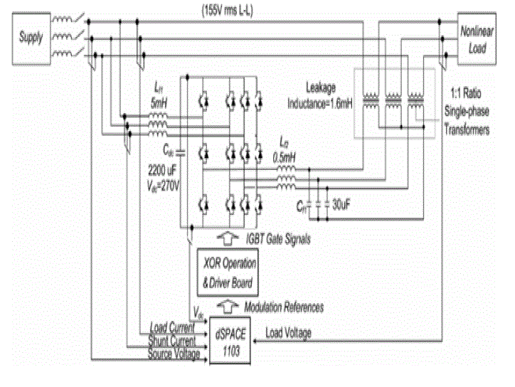 |
| Existing system circuit diagram |
PROPOSED SYSEM
|
| Only 9 switches are used here and switching losses are less in this method. The total harmonic distortion is less as shown in below Fig 5.2The same calculation can again be performed with no series compensation included. For the nine-switch UPQC, it just means the CF mode discussed in section set to zero and the transformer by passed. The former leads to a smaller dc link voltage, while the latter causes losses to be smaller, since large load current now does not flow through the nine-switch UPQC. |
| For comparison, values calculated for the back-to-back UPQC operating without series compensation are also included, with clearly show it having slightly lower losses under normal operating condition. |
| The lower losses here are attributed to the back-to-back UPQC using only six modulated switches for shunt compensation, while the nine-switch UPQC uses six up per modulated switches and three lower conducting switches. This would reverse when sag occurs, during which the back-to-back UPQC uses 12 modulated switches, while the nine-switch UPQC uses only nine, and hence producing lower losses. |
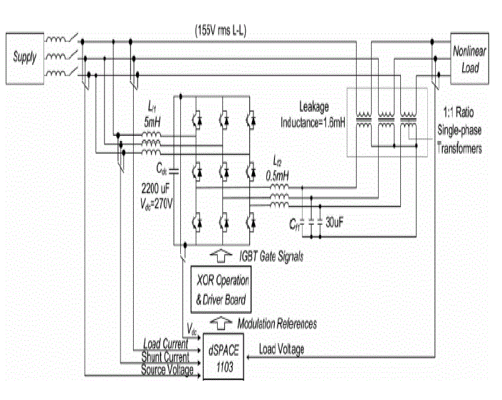 |
| Proposed system circuit diagram |
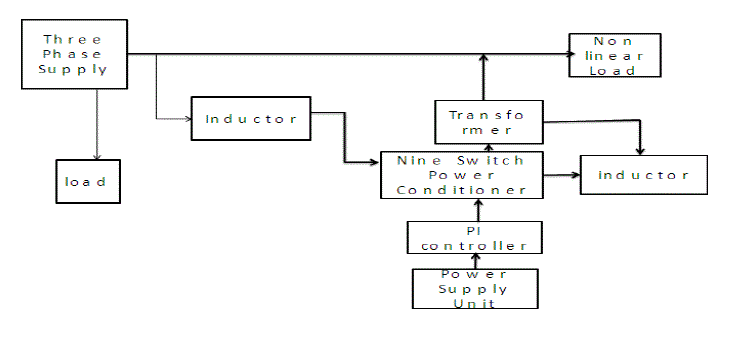 |
| Block Diagram of switched power conditioner |
SINUSOIDAL PWM-BASED CONTROL
|
| In order to mitigate the simulated voltage sags/swells in the test system of each mitigation technique, also to mitigate voltage sags/swells in practical application, a sinusoidal PWM-based control scheme is implemented, with reference to the POWER CONDITIONER. The control scheme for the POWER CONDITIONER follows the same principle. The aim of the control scheme is to maintain a constant voltage magnitude at the point where sensitive load is connected, under the system disturbance. The control system only measures the rms voltage at load point, for example, no reactive power measurements are required. The VSC switching strategy is based on a sinusoidal PWM technique which offers simplicity and good response. Since custom power is are relatively low-power application, PWM methods offer a more flexible option than the fundamental frequency switching (FFS) methods favoured in FACTS applications. Besides, high switching frequencies can be used to improve the efficiency of the converter, without incurring significant switching losses. Figure shows the POWER CONDITIONER controller scheme implemented in MATLAB. The POWER CONDITIONER control system exerts voltage angle control as follows: an error signal is obtained by comparing the reference voltage with the rms voltage measured at the load point. The PI controller processes the error signal and generates the required angle δ to drive the error to zero, for example, the load rms voltage is brought back to the reference voltage. |
| The filter blocks fundamental d-axis active component, and passes forward the harmonics and q-axis reactive component for further processing. In parallel a PI regulator is also added to act on the dc-link voltage error, forcing it in to zero by generating a small d-axis control reference for compensating losses. |
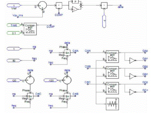 |
Control scheme for the test system implemented to carry out the POWER CONDITIONER simulations.
|
| The main parameters of the sinusoidal PWM scheme are the amplitude modulation index, ma, of signal v control, and the frequency modulation index, mf, of the triangular signal. The v controls in the Figure 4.1 are nominated as CtrlA, CtrlB and CtrlC. The amplitude index ma is kept fixed at 1 Pu, in order to obtain the highest fundamental voltage component at the controller output. The switching frequency mf is set at 450 Hz, mf = 9. It should be noted that, an assumption of balanced network and operating conditions are made. |
| The modulating angle δ or delta is applied to the PWM generators in phase A, whereas the angles for phase B and C are shifted by 240° or -120° and 120° respectively. It can be seen in Figure 4.1 that the control implementation is kept very simple by using only voltage measurements as feedback variable in the control scheme. The speed of response and robustness of the control scheme are clearly shown in the test results. |
SIMULATION MODEL AND RESULTS
|
| The increasing complexity in the power system, voltage sags and swells in power conditioner. The voltage sag is a short reduction voltage from nominal voltage, occurs in a short time, voltage swell is an increase in the r.m.s voltage from its nominal voltage; |
| They are bound to have a greater impact on the industrial customers. |
| Nine switch power conditioner (UPQC) appears to be an especially good solution in the current scenario. |
| Among these, the distribution static compensator and the dynamic voltage restorer are most effective devices, both of them based on the vsc principle this nine switch power conditioner. |
| The principle of working of Nine Switch power conditioner is shown in the following figure. |
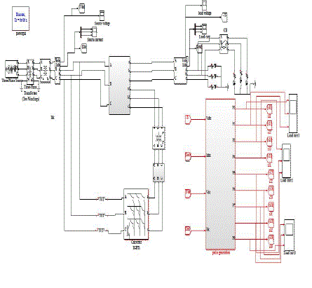 |
| Simulation Diagram For Nine Switch Power Conditioner |
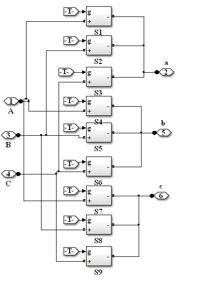 |
| Nine Switching Model |
| The simulation of gate pulse network reconfiguration method based on the graph theory algorithm is efficient and feasible for improving the bus voltage profile. The weak area is first determined before performing the appropriate switching action in network reconfiguration. The network reconfiguration solution is achieved by placing the weak area or the voltage sag sources as for as possible away from the main power supply. |
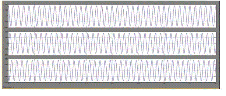 |
| Simulation Output Waveform for Input Source Current |
 |
| Simulation Waveform for Input Voltage |
 |
| Simulation Wave Form of Gate Pulse for Switches |
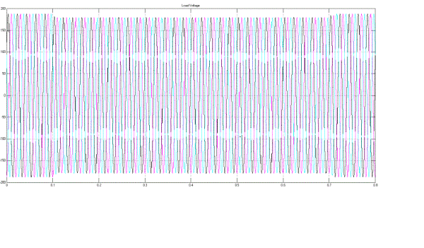 |
| Simulation Output Waveform for Voltage Sag |
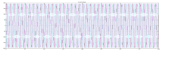
| The gate pulse has been generated and given for switches to turn on the switch those gate pulse are generated and given according to the gate pulse corresponding switch is turned ON and OFF which shown in the Fig 6.7 of waveform of gate pulse. The simulation output waveform for voltage sag at the time of voltage sag the transmission voltage is dropped down the voltage sag will be 220 v from phase to phase at the time voltage sag condition this creates the fault and it is overcome by 9 switch power conditioner as shown in the Fig |
 |
| Simulation Output Waveform for Voltage Sag Mitigation |
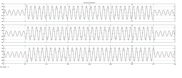 |
| Simulation Output Waveform for Load Current |
| The scope of waveform phase-to-phase rms voltage (v) is 240 and the frequency is 50 Hz. The base voltage is 240 v and the voltage measurement is phase to ground. The maximum frequency is 1000 Hz and the fundamental frequency is 60 Hz. When the 9 switch power conditioner is connected the voltage drop has been compensated after that normal phase to phase voltage 240 v has been maintained without any drop this minimize the fault at the transmission side. |
CONCLUSION
|
| This project has presented the power quality problems such as voltage dips, swells, distortions and harmonics. Compensation techniques of custom power electronic devices DVR was presented. The design and applications of nine switch power conditioner for voltage sags and comprehensive results were presented. A PWM-based control scheme was implemented. As opposed to fundamental frequency switching schemes already available in the MATLAB/SIMULINK, this PWM control scheme only requires voltage measurements. This characteristic makes it ideally suitable for low- voltage custom power applications. |
| The simulation results prove that the proposed network reconfiguration method based on the graph theory algorithm is efficient and feasible for improving the bus voltage profile. The weak area is first determined before performing the appropriate switching action in network reconfiguration. The network reconfiguration solution is achieved by placing the weak area or the voltage sag sources as far as possible away from the main power supply. This method is also efficient for network reinforcement against voltage sag propagation. By applying the proposed method, voltage sag at some buses can be completely mitigated while other buses are partially mitigated. |
| However, the voltage sag problem at the partially mitigated buses can be solved by placing other voltage sag mitigation devices. Although the reconfiguration process involves just a change is switching status, it solves majority of the voltage sag problems. The proposed method may assist the efforts of utility engineers in taking the right decision for network reconfiguration. The right decision can be taken after evaluating the benefits from line loss reduction and financial loss reduction due to implementation of network reconfiguration. |
References
|
- Ashcroft.D.L,(Sep.1985), “The static power converter committee—Some perspec-tives,” IEEE Trans. Ind. Applicat.,vol. IA-21, no. 5, pp. 1097–1098.
- Blaabjerg.F, Freysson.S, Hansen.H.H, and Hansen.S,(Jul. 1997), “A new op- timized space-vector modulation strategy for a componentminimized voltage source inverter,” IEEE Trans. Power Electron.,vol. 12, no. 4, pp. 704–714.
- Dehnavi.S.M.D, Mohamadian.M, Yazdian.A, and Ashrafzadeh.F,(Jun. 2010), “Space vectors modulation for nine-switch converters,”IEEE Trans. Power Electron., vol. 25, no. 6, pp. 1488–1496.
- Gao.F, Zhang.L, Li.D.P. , Loh.C, Tang.Y, and Gao.H,(Sep. 2010), “Optimal pulsewidth modulation of nine-switch converter,”IEEE Trans. Power Electron., vol. 25, No. 9, pp. 2331–2343.
- Han.B, Bae.B, Kim.H, and Baek.S,(Jan. 2006), “Combined operation of uni- fied power-quality conditioner with distributed generation,”IEEE Trans. Power Delivery, vol. 21, no. 1, pp. 330–338.
- Jones.M, Vukosavic.S.N, Dujic.D, Levi.E, and Wright.P,(Sep. 2008), “Five-leg inverter PWM technique for reduced switch count twomotor constant power applications,”IET Proc. Electric Power Applicat., vol. 2, no. 5, pp. 275–287.
- Johal.H and Divan.D, (Nov/Dec. 2007), “Design considerations for series-connected dis-tributed FACTS converters,” IEEE Trans. Ind. Applicat., vol. 43, no. 6, pp. 1609–1618.
- Khadkikar.V and Chandra.A,(Oct. 2008), “A new control philosophy for a uni- fied power quality conditioner (UP6.QC) to coordinate load-reactive power demand between shunt and series inverters,”IEEE Trans. Power Del., vol. 23, no. 4, pp. 2522–2534.
- Kominami.T and Fujimoto.Y, (2007) “A novel three-phase inverter for indepen- dent control of two three-phase loads,” in Proc. IEEE-Ind. Applicat. Soc. (IAS)s, pp. 2346–2350.
- Loh.P.C, Blaabjerg.F, Gao.F, Baby.A, and Tan.D.A.C,(Nov./Dec. 2008), “Pulsewidth modulation of neutral-point-clamped indirect matrix converter,”IEEE Trans. Ind. Applicat., vol. 44, no. 6, pp. 1805–1814.
- Ledezma.E, McGrath.B, Munoz.A, and Lipo.T.A,(Sep./Oct.2001) “Dual ac-drive system with a reduced switch count,” IEEE Trans. Ind. Applicat., vol. 37, no. 5, pp. 1325–1333.
- Liu.C, Wu.B, Zargari.N.R, Xu.D, and Wang.J,(May 2009) “A novel three- phase three-leg ac/ac converter using nine IGBTs,” IEEE Trans. Power Electron., vol. 24, no. 5, pp. 1151–1160.
- Lee.T.L, Li.J.C, and Cheng.P.T, (May 2009)“Discrete frequency tuning active filter for power system harmonics,” IEEETrans.PowerElectron.,vol.24,no.5, pp. 1209–1217.
- Li.Y, Vilathgamuwa.D.M, and Loh.P.C,(Nov./Dec. 2005) “Microgrid power quality en-hancement compensator,”IEEETrans. Ind.Applicat.,vol.41,no.6,pp.1707–1719.
- Ojo.O,(Dec. 2004) “The generalized discontinuous PWM scheme for three-phase voltage source inverters,” IEEE Trans. Ind. Electron., vol. 51, no. 6, pp. 1280–1289.
|