In recent years, power generation utilizing solar power or wind power has been being great attractive for effective utilization of electrical energy. In Order to protect the natural environment on the earth, the development of clean energy without pollution has the major representative role in the last decade. By dealing with the issue of global warming, clean energies, such as fuel cell (FC), photovoltaic, and wind energy, etc., have been rapidly promoted.Standalone photovoltaic (SAPV) systems are widely used in remote areas after development of photovoltaic cell industry in recent years. A PV cell has an exponential relationship between current and voltage, and the maximum power point (MPP) occurs at the knee of the curve. In this paper a photovoltaic array is used to run a DC motor using a dc-dc converter. The gating signal to the dc-dc converter is giving using soft switching technique. The simulink model of the PV array connected to dc motor using a dc –dc converter is developed in MATLAB and the outputs are observed.
Keywords |
| Photovoltaic array, Soft Switching, ambient temperature, irradiation level. |
INTRODUCTION |
| In recent years the population of India is being increased rapidly. The utilization of power has become very important
in every humans life. Any work a human does is directly or indirectly related to power. And people now a days are
developing many equipments and machines in order to make their work more easier. And hence there is a great demand
for electrical energy. The power generating stations are unable to meet the demand, due to which the people are facing
a great power crisis. In addition to it there are many remote places where the electrical power cannot be transmitted.
Hence there is great need to utilize the non-renewable energy resources(like fuel cell, wind energy, solar energy etc.,)
for power generation. |
| In this paper an efficient attempt is made for using the non-renewable energy resource(solar energy) as an voltage
source input i.e. the output voltage of the photovoltaic array is used as an input to run the load. In this paper the load
and the source are separated by a dc-dc converter. The gating signals to the converter are giving using soft switching
technique which has the advantage of reducing are eliminating the commutation losses. The converter used here has an
efficiency of about 93 percent. In this paper the simulink model of the pv array connected to dc motor separated by a
dc –dc converter is developed in Matlab and the outputs are presented. The block diagram shown below gives a basic
idea of the paper: |
| The above figure shows the basic block diagram of the project. The small output voltage of the PV array is given to the
boost chopper where the voltage is boosted. This voltage is fed to the dc to dc converter where the efficient conversion
is made at high efficiency. This improved dc voltage is fed to the dc motor which makes the motor to run. |
PHOTOVOLTAIC ARRAY MODELING |
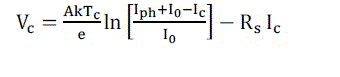
| PV arrays are built up with combined series/parallel combinations of PV solar cells, which are usually represented
by a simplified equivalent circuit model as shown below. |
| The output voltage of PV cell is a function of the photocurrent that mainly determined by load current depending on the
solar irradiation level and is given by: |
 (1) (1) |
| Where |
| e : electron charge (1.602×10⁻¹⁹C). |
| k : Boltzmann constant(1.38×10⁻²³ J/°K). |
| Ic : cell output current, A. |
| Iph : photocurrent, function of irradiation level and junction temperature (5 A). |
| Io : reverse saturation current of diode (0.0002 A). |
| Rs : series resistance of cell (0.001 Ω). |
| Tc : reference cell operating temperature (20 °C). |
| Vc : cell output voltage, V. |
| The above gives the voltage of a single solar cell, the full array voltage is obtained by multiplying the voltage of single
solar cell with the number of cells connected in series. |
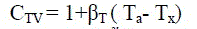
| The operating temperature of the solar cell as a function of solar irradiation level and ambient temperature. The cell
output voltage and cell photocurrent are affected by the ambient temperature Ta.. These affects are represented in the
model by temperature coefficients CTV and CTI for cell output voltage and cell output current, respectively, as: |
 (2) (2) |
 (3) (3) |
| where,βT =0.004 and γT = 0.06 for the cell used and Ta=20oC is the ambient temperature during cell testing.
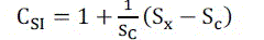
A change in solar irradiation level causes a change in the value of cell photocurrent and cell operating temperature
,which in turn affects the cell output voltage. Thus the change in operating temperature and photocurrent due to the
change in the solar irradiation level can be given via two constants, CSV and CSI, which are correction factors for the
change in the cell voltage and cell current respectively: |
 (4) (4) |
 (5) (5) |
| Where SC is the standard solar irradiation level during cell testing and SX is the new level of solar irradiation. The
change in temperature, ΔTC occurs because of the change in the solar irradiation level and is obtained using the
equation |
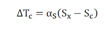 (6) (6) |
| Using the above correction factors the new values of the cell output voltage and the photocurrent are obtained for the
new temperature Tx and solar irradiation Sx as follows: |
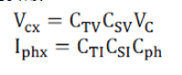 |
| Where VC and Iph are the benchmark reference cell output voltage and reference cell photocurrent respectively. |
PVA MODELING FOR SIMULINK |
| The general block diagram of the PVA model for simulink is shown below. |
| The figure above shows the simulink model of the PV array whose output after simulation is obtained as 83volts. |
DC-DC CONVERTER |
| A bidirectional dc to dc converter is used for the better performance of the load. The isolated bidirectional dc to dc
converter consists of a boost chopper circuit and a full bridge type LLC converter for isolation. The boost chopper is
used to boost the output voltage of the photovoltaic array.
The bidirectional boost chopper circuit consists of a input capacitor Cchop, input inductor Lchop and two IGBT switches
Qchop1,Qchop2. The full bridge type LLC converter consists of a DC link capacitor C1, four switches for full bridge in
primary side, resonant capacitor Cr, and inductor Lr, transformer, four switches in the secondary side and a smoothing
capacitor Cbus. |
| The isolated bidirectional dc –dc converter used is shown below. |
| In general the switching of the bidirectional dc – dc chopper circuit shows hard switching and in order to prevent from
short circuit there is dead time for on and off of switch Qchop1 and Qchop2. The pulse width modulation (PWM) control is
adopted for the bidirectional boost chopper circuit. The isolated bidirectional dc to dc converter is driven with duty of
nearly 50% to attain best efficiency. Dead time for the switches Q1,Q4,Q5,Q8 and Q2,Q3,Q6,Q7 is set up. If the duty of
isolated bidirectional dc to dc converter is fixed, the current and voltage control isn’t required. |
| The operation principle for the isolated bi-directional DC-DC converter is discussed below. The operation of the
isolated bi-directional dc to dc converter can be explained in six modes as follows: |
| Mode 1: The switches Q1, Q4, Q5, and Q8 are on. The resonant voltage of the capacitor Cr is positively charged in
this moment and then resonant capacitor Cr starts to discharge. After that, the resonant voltage of capacitor Cr crosses
zero and completes to charge negatively. The current of inductor Lr is approximately zero. |
| Mode 2: The switches Q1, Q4, Q5, and Q8 turn on since the resonant current of the inductor Lr is zero. For that
reason, the ZCS operation is realized due to no current switching. Each of the switches turns off. After that, they are in
the dead time period. |
| Mode 3:The beginning of this mode starts from the dead time period. All switches are in the off state. After finishing
the dead time period, the switches Q2, Q3, Q6, and Q7 turn on. At this time, the ZCS operation is achieved since the
switch current gradually rises up by the resonant capacitor Cr and inductor Lr. In this moment, the resonant voltage of
the capacitor Cr shows the negative voltage. |
| The figures below (fig5 and fig 6) show the operation stages for discharge and each of the voltage and current
waveforms in discharging time for the isolated bi-directional dc to dc converter. |
| Mode 4: The switches Q2, Q3, Q6, and Q7 turn on and then the resonant capacitor Cr starts to discharge with resonant.
After that, the resonant capacitor Cr charges positively due to the resonant. In other words, the current and voltage of
the resonant capacitor Cr and inductor Lr change in contrast to Mode1. |
| Mode5: The resonant current of inductor Lr becomes approximately zero, and then the switches Q2, Q3, Q6, and Q7
turn on. Accordingly, the ZCS operation is realized. After that, each of the switches turns off and the mode moves to
next mode. |
| Mode6: In the beginning of this mode, all switches are in the off state. Finishing the dead time period, the switches Q1,
Q4, Q5, and Q8 turn on. At this moment, the ZCS operation is realized since the current gradually rise up with the
resonant. After turning on,the mode moves to Mode1. |
| A output voltage of the converter is given to the motor and the output is observed. The output is given back for the
required operation of the motor. The error voltage is given to the pi duty controller where the duty cycle is obtained.
The obtained duty cycle is given to the PWM generator which in turn provides the gating signal for the boost chopper
and thus the cycle repeats. |
SIMULATION AND RESULTS |
| The simulation circuit for a dc to dc converter connected to a motor load fed by a photovoltaic cell is shown below: |
| The simulink diagram shown above is the complete model of a PV array connected to a dc motor through a dc to dc
converter. |
| The figure shown below represents the output waveforms of the dc motor. The first waveform represents the speed of
the motor for the time(t). |
| The second waveform represents the armature current of the dc motor for a particular time(t). And the third waveform
represents the torque of the dc motor for a particular time(t). |
CONCLUSION |
| The simulation of the isolated bi directional dc to dc converter connected to a motor load fed by a photovoltaic cell is
carried. This is an efficient way of utilizing the non renewable energy resources for domestic appliances where there is
no availability of power supply. |
| Here the use of the bidirectional dc to dc to converter is advantageous as it enhances the signal and helps in boosting
the voltage obtained from the output of the photovoltaic array. The output of the PV array is a low voltage which can
be boosted up to a required level using the converter. This is the great advantage of this project as the appliances can be
run with less number of solar cells. This work can be extended to even ac motors by introducing an inverter circuit at
the load side. Hence this can be best option at the remote places where there is no way to transmit the power. |
Figures at a glance |
 |
 |
 |
 |
| Figure 1 |
Figure 2 |
Figure 3 |
Figure 4 |
 |
 |
 |
 |
| Figure 5 |
Figure 6 |
Figure 7 |
Figure 8 |
|
| |
References |
- Wei. Chen and Zhengyu Lu. ?A Novel ZVS Set-up Push-Pull Type Isolated LLC Series Resonant Dc-Dc Converter for UPS Systems andIts Topology Variations,? IEEE Applied Power Electronics Conference and Exposition (APEC)., pp. 1073-1078, Feb. 2008
- Greg Stahl, Miguel Rodriguez, and DraganMaksimovic, ?A High- Efficiency Bidirectional Buck-Boost DC-DC Converter,? IEEE AppliedPower Electronics Conference and Exposition (APEC)., 1362-1367, Feb. 2012
- Seung-Ryul Moon, Ki-Chang Lee, Jong-Moo Kim, Dae-Hyun Koo, ?Closed-Loop Regenerative Efficiency Testing with Electric VehicleBidirectional Dc-dc Converter,? IEEE Applied Power Electronics Conference and Exposition (APEC)., 2461-2466, Feb. 2012
- Seung-Ryul Moon, Ki-Chang Lee, Jong-Moo Kim, Dae-Hyun Koo, ?Novel Moduration Method of a Three-Level Isolated Full-Bridge LLCResonant DC-DC Converter for Wide-Output Voltage Application,? IEEE Power Electronics and Motion Control Conference (EPC/PEMC).,DS2b.11-1-DS2b.11-7
- I.H. Altas, and A.M. Sharaf,? A Photovoltaic Array Simulation Model for Matlab-Simulink GUI Environment,? \
- Dr. Abu Tariq, Mohammed Asim,? Simulink based modeling, simulation and performance Evaluation of an MPPT for maximum powergeneration on resistive load,? 2011 2nd International Conference on Environmental Science and Technology IPCBEE vol.6 (2011) © (2011)IACSIT Press, Singapore
|