Research & Reviews: Journal of Material Sciences
ISSN:2321-6212
ISSN:2321-6212
Xiaowen Hu*, Yifan Feng
SCNU-TUE Joint Lab of Device Integrated Responsive Materials (DIRM), National Centre for International Research on Green Optoelectronics, South China Academy of Advanced Optoelectronics, South China Normal University, Guangzhou 510006, China
Received: 21-Dec-2023, Manuscript No. JOMS-23-123244; Editor assigned: 26- Dec-2023, PreQC No. JOMS-23-123244 (PQ); Reviewed: 09-Jan-2024, QC No. JOMS-23-123244; Revised: 16-Jan-2024, Manuscript No. JOMS-23-123244 (R); Published: 23-Jan-2024, DOI: 10.4172/2321-6212.12.1.001
Citation: Hu X, et al. A Review on Recent Progress in Circularly Polarized Light Photodetector. RRJ Mater Sci. 2024;12:001.
Copyright: © 2024 Hu X, et al. This is an open-access article distributed under the terms of the Creative Commons Attribution License, which permits unrestricted use, distribution, and reproduction in any medium, provided the original author and source are credited.
Visit for more related articles at Research & Reviews: Journal of Material Sciences
Circularly Polarized Light (CPL) has irreplaceable advantages in optoelectronic fields such as magnetic recording, quantum computing and optical communications. Circularly polarized light is a good carrier of information because of its regularity along the direction of propagation. In order to fully exploit the functions of CPL in these fields, circularly polarized light photodetectors are necessary. Conventional CPL photodetectors require complex optics and can only indirectly detect circularly polarized light, which hinders device miniaturization and application promotion. Therefore, direct CPL photodetectors have received more attention in recent years. Up to now, CPL photodetectors have been significantly developed. In this paper, we review the recent progress of CPL photodetectors based on chiral materials and chiral hypersurfaces that can convert optical field chirality into directional photocurrents, and introduce the potential applications of CPL photodetector, and finally we discussed the challenges and opportunities that CPL photodetectors are expected to face in the future.
Circularly polarized light; Photodetector; Direct detection; Chiral materials; Chiral hypersurfaces
In recent years, Circularly Polarized Light (CPL) has generated substantial scientific interest in quantum computing, spintronics 3D display chiral biosensing and magnetic recording [1-11]. CPL is a superposition of two linearly polarized light waves of equal frequency, mutually perpendicular vibrational directions, and constant phase difference. Unlike natural light, the light vector of CPL fluctuates regularly during propagation. Specifically, the electric field vector moves perpendicular to the propagation direction in a clockwise or counterclockwise spiral trajectory. The direction of rotation of the light vector determines the classification of CPL into left-rotating and right-rotating light (L-CPL or R-CPL). The creation of a high-performing CPL photodetector is a necessary requirement for CPL-based applications. Conventional CPL photodetector utilize a quarter-wave wafer to convert circularly polarized light into linearly polarized light [12-14]. This conversion allows for indirect detection of CPL with the use of a polarizer and conventional photodetector. Nevertheless, the unfeasible size and intricate optical polarization elements associated with this approach inhibit miniaturization and integration of photodetector devices. Therefore, the need to develop a miniaturized and integrated device has driven the development of direct detection of CPL. According to the different working mechanisms, there are two main ways to realize the direct detection of CPL. The first approach is a circularly polarized photodetector based on chiral materials [15, 16]. A chiral material is one in which the molecule has enantiomers, and the material itself cannot coincide with its mirror image. Due to the circular dichroism of chiral materials, which exhibits different light absorption coefficients for LCP and RCP, circularly polarized photodetectors based on chiral materials generate differentiated photocurrents under the irradiation of LCP and RCP, thus enabling the detection of CPL. The second approach is by creating chiral hypersurfaces to detect CPL [17,18]. The detection mechanism is based on the enhancement of CPL with different spins by a chiral supersurface coupled with the plasmon resonance effect, which generates different photocurrents under the irradiation of CPL with different spins. Here, we revisit the research progress of CPL photodetectors in recent years, including CPL photodetectors based on different mechanisms and materials, and their potential applications. Finally, a summary on the ongoing researches along with their potential and challenges are provided toward the end.
Operating mechanisms for photodetector
The current detection mechanism of photodetectors can be photoelectric effect, photovoltaic effect and photothermal-electric effect [19-22]. The photoelectric effect refers to the fact that in a dark environment, due to the low concentration of carriers in the semiconductor, the photoconductor will exhibit high resistance. When the photoconductor is exposed to light, the electrons in the valence band jump to the conduction band after absorbing the energy of the photons, thereby generating carriers in the semiconductor layer, resulting in a reduction in the resistivity of the photoconductors. Whereas the photovoltaic effect is realized with the help of PN junctions. A strong built-in electric field exists in the potential barrier region of the PN junction, and the electrons in the P region enter the N region and the holes in the N region enter the P region, which increases the potential at the P-terminal end and decreases the potential at the N-terminal end, generating a photogenerated electromotive force at both ends of the PN junction. The photo thermoelectric effect is the generation of hot carriers in the material under light illumination, in which the concentration of hot carriers and the temperature gradient to drive the carriers to directional motion and thus produce a photoelectric response. The various mechanisms mentioned above correspond to different photodetector structures, which can be classified as photoconductors, photodiodes and phototransistors [15].
Indicators of performance for CPL photodetectors
Although photodetectors based on semiconductor materials may have different operating mechanisms, they generally require the use of similar parameters to characterize their performance. There are several key parameters used to evaluate the performance of CPL photodetectors, including Photosensitivity (P), Responsivity (R), External Quantum Efficiency (EQE), Specific detectivity (D*), Linear Dynamic Range (LDR),the anisotropy factor of responsivity (gres)and response speed, which are summarized as follows [23].
1. Photosensitivity (P) of a photodetector indicates the increase in the signal of the photodetector after receiving light, and its value is defined as follows.
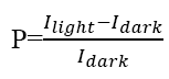
Where Idark denotes the dark current of the device in a dark environment and Ilightdenotes the photocurrent generated by the device in light.
2. Responsivity (R) quantifies the ability of a CPL photodetector to convert light into current, and its value is defined as follows.
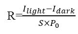
where P0denotes the optical power and S represents the area of light irradiated by the device.
3. External Quantum Efficiency (EQE) is defined as the ratio of the number of photo-generated carriers that actually enhance the drain current to the number of photons irradiated to the device and its value can be calculated using the following equation [23] .
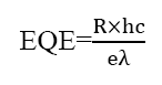
Where h is Planck constant, R is the responsivity, c is the speed of light, e is the fundamental unit of charge, and λ is the wavelength of maximum absorption.
4. Specific detectivity (D*) characterizes the sensitivity of the CPL photodetector, whose value can be calculated by the following formula [24, 25].
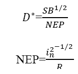
Where B denotes the bandwidth, NEP denotes the Noise Equivalent Power, and  refers to the RMS value of the noise current.
5. Linear Dynamic Range (LDR) is defined as the range of illumination intensities in which the current response of the photodetector is linearly proportional to the light intensity, whose value is defined using the following equation:
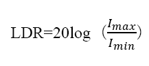
Where Iminand Imaxdenote the maximum and minimum current, respectively.
6. The anisotropy factor of responsivity (gres) indicates the ability of a CPL photodetector to distinguish between L-CPL and R-CPL, the value of which can be calculated by the following equation
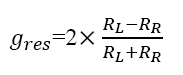
Where RL and RR denotes the responsiveness of the CPL photodetector to L-CPL and R-CPL, respectively.
7. The response speed of a photodetector is characterized as the rise time (trise) and fall time (tdecay) of the current signal under the excitation of an optical signal. The rise time (trise) is defined as the time required for the photocurrent to rise from 10% of its maximum value to 90% of its maximum value under incident light. In contrast, the fall time (tdecay) is defined as the time required for the photocurrent to fall from 90% of the maximum value to 10% of the maximum value under the removal of the incident light [26].
CPL photodetector based on chiral materials
Organic semiconductors have a wide range of applications in optoelectronics due to their large absorption coefficients and good solution process ability [27-30]. Organic semiconductors can be used as active layers in photodetectors with detection ranging from the ultraviolet to the infrared region due to their tunable optical energy gap and carrier transport properties [31-35]. Organic semiconductors, combined with chirality, have excellent photoelectric properties [36-38], which can therefore be used as active layers in CPL photodetectors. For example, reported the first phototransistor based on an organic light-emitting diode that can selectively detect R-CPL and L-CPL [39]. Figure 1a shows the molecule structure of chiral small molecules (+)-1-aza [6] helicene and (-)-1aza [6] helicene. They realized the detection of CPL based on OFET of chiral small molecules (+)-1-aza [6] helicene and (-)-1aza [6] helicene, as shown in Figure 1b. The specific response of the device to the direction of CPL polarization is directly related to the helical chirality of the molecules. The device shows significantly different photocurrents between RCP and LCP illumination, with a response at 365 nm of 10 mAW−1(Figure 1c). This can be attributed to the fact that helicenes with helical chiral and fully conjugated structures not only bring strong chirality to the molecule, but also moderately increase the charge transport efficiency. In addition to organic molecules, conjugated polymers can also be used in CPL photodetectors due to their good film formation, large-scale process ability, strong mirror circular dichroism and excellent photovoltaic properties [3,40-43]. reported intrinsic heterojunction photodetector devices based on the achiral polymer polythiophene derivative P3CT and the chiral small molecule 1,1'-binaphthyl BN [44]. As shown in Figure 1d, the authors utilized intermolecular hydrogen bonding interactions to transfer the chirality of the chiral small molecules onto the non-chiral polymer and formed a unique active ayer structure by thermal annealing. The upper layer of the device is a microcrystalline layer enriched with chiral small molecules, and the lower layer is a hybrid layer enriched with chiral small molecules (Figure 1e). As illustrated in Figure 1f, photodiodes show differential photocurrents under irradiation with different chiral lights. The gphof the 49/R-50 and 49/S-50 heterojunction based photodiodes reaches 0.1. In order to further improve the device performance, there is a need to develop more chiral organic semiconductor with high performance. Realized the detection of CPL using nanowire-constructed OFETs by preparing nanowires of n-type semiconductor chiral perylenimide (CPDI-Ph) S-/R-42 by self-assembly in solution [38]. Figure 1g shows that molecular structures of (S)-CPDI-Ph and (R)-CPDI-Ph and crystal structures of homochiral (S)-CPDI-Ph NWs. As shown in Figure 1h, the CPL photodetector has an EQE maximum of 8.81 × 10⁴% with R up to 334 A W−1under 460 nm monochromatic light at a gate voltage of 82 V. Prepared the first realization of porphyrin-based chiral photovoltaic films[45].

Figure 1: (a) Molecular structure of (+)-1-aza [6]helicene and (−)-1-aza [6]helicen, where (+)-1-aza [6]helicene is the right-handed (P or +) enantiomeric and (−)-1-aza [6]helicene is the left-handed (M or −) enantiomeric; (b) The device structure of the CPL phototransistors; (c) Transfer characteristic curve of the phototransistors based on (+)-1-aza [6] helicene in the dark or under CPL illumination (λ=365 nm, power=10 mWcm2). Reproduced with permission from ref copyright 2021, Nature Publishing Group; (d) Schematic explanation of P3CT and BN hybrid system; (e) Device structure of the photodiode based on the P3CT/BN hybrid thin film; (f) Photo response characteristics of P3CT/BN hybrid thin-film photodiodes with a thickness of 550 nm under repeated on/off modulation of incident CPL. Reproduced with permission Copyright 2019, WILEY‐VCH Verlag GmbH & Co. KGaA, Weinheim; (g) structures of (S)-CPDI-Ph and (R)-CPDI-Ph; (h) Schematic diagram of CPL generation in the experiment and IDS–VG characteristics in dark or under CPL illumination (λ =460 nm, power=50 µW cm−2) for OPTs. Reproduced with permission copyright 2017, WILEY‐VCH Verlag GmbH & Co. KGaA, Weinheim.
As presented in Figures 2a-c, the non-chiral porphyrin nuclei gained chirality upon assembly in a metal-organic backbone (MOF) film, and the tight stacking and crystallization order of the porphyrin nuclei in the MOF film also led to excellent photovoltaic properties, especially under 455 nm light irradiation. The device obtained g_res of 4.3 × 10⁻⁴ demonstrating that assembly-modulated chiral induced porphyrins can be combined with a wide range of chemically functionalized porphyrins by various methods. It is believed that a similar approach to prepare chiral materials can be applied to similar materials of phthalocyanine, dinaphthalene embedded benzodiimide and benzodithiophene. Introduced a backbone merging methodology by deforming a dinaphthalene embedded benzene diimide (PDI) core with four thickened heteroaromatic compounds to form neighboring-π-extended PDI bis[7] heterospiroenes as shown in Figure 2d [46]. The PDI bis-spiroenes inherit the high asymmetry factor of the spiroene backbone. The extended π-planar system simultaneously maintains a high level of charge transport properties (Figure 2e). In addition, the neighboring-π-extension of the PDI backbone provides Near-Infrared (NIR) light absorption and bipolar charge-transport capabilities, endowing the corresponding organic phototransistors with high responsivity of 450 mA W−1 and 120 mA W−1 in p-type and n-type modes, respectively, and a high EQE of up to 89% under NIR light irradiation, as presented in Figure 2f. Conventional photodetectors require an external bias voltage for operation, which is not conducive to large-area integration with other components and results in unnecessary energy consumption. Therefore, self-powered photodetectors that combine miniaturization and low energy consumption have become the focus of researchers' attention. Demonstrated a self-powered heterojunction photodiode photodetector based on a mixture of chiral ProSQ-C6 and the conventional fullerene acceptor phenyl-C61-butyric acid methyl ester (PCBM) with a mass ratio of 2:3 [47]. Figures 2g and 2h show the molecular and device structures, respectively. As shown in Figure 2i, the results showed that the (R,R)-enantiomers have preferential sensitivity to L-CPL and (S,S)-enantiomers have preferential sensitivity to R-CPL. The current asymmetry was 0.08 ± 0.02 for (R,R)-devices and reached -0.10 ± 0.01 for (S,S)- devices.

Figure 2: (a) Molecular structure of R-MeBINOL-PorDC; (b) Structure of the optimized Zn(R-MeBINOL-PorDC) SURMOF; (c) DC current versus time at a voltage of 2 V when the sample is irradiated with light of 640 nm, 530 nm, 455 nm, 400 nm and 365 nm wavelength, respectively. Reproduced with permission from copyright 2022, WILEY‐VCH Verlag GmbH & Co. KGaA, Weinheim; (d) Molecular structure of tetraindole-fused PDIs; (e) R and D* of 3a-P-based OFETs under the NIR light irradiations in p-type(λ=730 nm, 540 μW cm−2); (f) Maximum R, P, EQE, and D* values of 3a-P-based OFETs under the NIR light irradiations(λ =730 nm, 540 μW cm−2). Reproduced with permission from copyright 2021, Nature Publishing Group; (g) Structure of ProSQ-C6; (h) A schematic diagram of the device architecture; (i) Photocurrent anisotropy calculated (g1sc) under 543 nm CPL irradiation. Reproduced with permission from ref [47], Copyright 2019, WILEY‐VCH Verlag GmbH & Co. KGaA, Weinheim.
However, all the devices fabricated using a single chiral semiconductor as the active layer can only achieve a preferred response to one polarization state of CPL, which greatly hampers the ability of CPL photodetectors to be integrated with different functions of other devices. To address this problem, Utilized CPL-induced nonchiral conjugated polymers to construct OFETs for direct detection of CPL. The L-CPL-induced devices were irradiated with L-CPL and R-CPL irradiation with responsivity of 1.86 × 10⁻⁵ A W−1and 9.42 × 10⁻⁶ A W−1, D* values of 7.44 × 10⁷Jones and 4.21 × 10⁷ Jones, and EQE of 12 × 103% and 8.16 × 10⁻⁴%, respectively. Figure 3a. proposed a programmable CPL phototransistor based on a poly(9,9-dihexylfluorene-alt-benzothiadiazole) (F6BT)/poly(3-hexylthiophene) (P3HT) bilayer structure, as 11shown in Figure 3b [48]. The molecular structure is shown in Unlike all previous reports in the literatures, induced by non-contact CPL, the CD signal intensity of F6BT films increased with induction time as monochromatic CPL action was prolonged over a certain time range and showed a preferential response to CPL with the same chirality as that of the induced chiral light Figure 3c. More importantly, the CD signal of the F6BT films can be directly inverted by modulating the polarization state of the CPL. The inversion of the F6BT chirality can be attributed to the fact that the M-helical conformation predominates in the system in the L-CPL-induced F6BT. Comparatively, in R-CPL-induced F6BT, the P-helical conformation dominates in the system Figure 3d. Thanks to the good carrier transport properties of the P3HT layer, the maximum responsivity and the gres values of the device reach 2.76 A W−1 and 0.425, respectively. The team proposed and experimentally demonstrated for the first time a novel CPL photodetector based on an achiral organic semiconductor, which provides an effective method for using a single realization for preferential response to oppositely chiral CPL.

Figure 3: (a) Chemical structure of F6BT and P3HT; (b) Schematic illustration of the device structure; (c) CD spectra and gCD of the F6BT films irradiated with L- or R-CPL as a function of induction time; (d) Schematic illustration of the mechanism that the optical activity of F6BT films can be programmed by L-CPL and/or R-CPL. Reproduced with permission from copyright 2022, American Chemical Society; (e) TEM and schematic of the chiral PT nanowire structure; (f) schematic of the setup of CPL detection; (g) Diagram of electron excitation and recombination under the effect of chirality generated OAM. Reproduced with permission from copyright 2020, American Institute of Physics.
At present, the detection mechanism of CPL by CPL photodetector based on chiral materials mainly consists of differential absorption of left-handed and right-handed CPL and chirally generated Orbital Angular Momentum (OAM). Constructed a CPL photodetector based on chiral polythiophene nanowires possessing strong orbital angular momentum to explore the intrinsic mechanism [49]. The TEM and schematic of the chiral PT nanowire structure is illustrated in Figure 3e. Figure 3f presents the test optical path and device structure. The authors hypothesize that the chiral-induced electron spin-orbit angular momentum may have an important contribution to CPL detection in the case that the difference in absorption of L-/R-CPL by chiral molecules does not contribute much to the anisotropy of each photocurrent of the device. The authors suggest that chirality enhances spin-orbit coupling in organic optoelectronic materials, which in turn leads to spin-up and spin-down energy level cleavages Figure 3g. This effect further leads to lower dissociation energies and smaller complexation rates of the photo generated excitons of one of the polarized states of the CPL in a material with a given chirality, leading to higher photo generated currents relative to those in devices based on the opposite chirality, and ultimately to higher asymmetric currents in the devices. This study provides an important idea to explain the origin of asymmetric currents in CPL photodetector.
However, since chiral semiconductors inherently have the disadvantage of low responsivity to CPL of different chirality, it is necessary to explore other ways to fabricate high-performance CPL photodetectors. Cholesteric liquid crystals have attracted the attention of researchers [50]. As a self-assembled one-dimensional photonic crystal material, cholesteric liquid crystals can be widely used in light-emitting diodes, reflection-free lasers, tunable color filters, and light diffraction gratings for reflective devices [51-53]. Cholesteric liquid crystals have a special light modulation function, and their selective reflection of light can easily achieve the role of recognizing CPL with different spins. Cholesteric liquid crystals selectively reflect CPL of the same chirality as their own, and selectively transmit CPL of the opposite chirality to their own [54]. At the same time, cholesteric liquid crystals are simple and inexpensive to prepare, and through easy to integrate into devices [55-58]. Thus, one of the approaches to realize high-performance CPL photodetectors is through the combination of cholesteric liquid crystals and achiral organic semiconductors. Assembled a cholesteric liquid crystal film in a near-infrared organic phototransistor with a non-chiral narrow bandgap polymer PODTPPD-BT as the active layer to prepare a near-infrared CPL direct photodetector, which showed a remarkable responsiveness and distinguishability to CPL, with a dissymmetry factor as high as 1.9 [59]. The device structure is shown in Figure 4. The R-value of this device at 830 nm was about 300 A W−1 at 830 nm with an EQE of 4.5 × 10⁴%.

Figure 4: Schematic of the device structure of NIR CPL-OPTRs under circularly polarized NIR illumination and chemical structure of PODTPPD-BT. Reproduced with permission. Reproduced with permission from ref [59], Copyright 2020, WILEY‐VCH Verlag GmbH & Co. KGaA, Weinheim.
In addition to the combination of cholesteric liquid crystals and organic semiconductors for the fabrication of CPL photodetectors, chiral organic and inorganic hybrid perovskite have attracted much attention because of their combination of good photoelectric properties and differentiation between different chiral lights. Organic-inorganic halide perovskite have a wide range of applications in the field of optoelectronic devices because of their high carrier mobility, long carrier lifetime, low defect density and high light absorption coefficient [60-62]. Their direct bandgap, high light absorption capacity, and tunable emission wavelength properties make perovskite promising candidates for optoelectronic applications [63-67]. By combining chirality with organic-inorganic perovskite, makes chiral organic-inorganic halide perovskite favorable candidates for active layers in CPL photodetectors. To prepare CPL photodetectors with excellent performance, the active layer is required to respond preferentially to light of a specific spin nature, in addition to high CPL absorption and high electron mobility [29, 68-70]. Accordingly, chiral molecules have a natural advantage in responding to light of a specific spin. In contrast to organic molecules, inorganic compounds usually show high carrier mobility since carriers are transported within the energy bands of inorganic compounds. Therefore, it would be highly feasible to use materials that combine chiral molecules and inorganic compounds for the active layer of CPL photodetectors. Chiral organic-inorganic halide perovskite synthesized by incorporating chiral organic molecules into inorganic halide perovskite combine excellent optoelectronic properties with a preferential response to specific chiral light. The first CPL photodetector based on chiral organic-inorganic hybridized perovskite (α−PEA)2PbI4 was fabricated by [71]. They combined the CPL-sensitive absorption properties of chiral α-Phenylethylamine (α-PEA) with the efficient charge transport of the inorganic framework. Resulting in R values of 797 mA W−1, D*values of 7.1 × 10¹¹ Jones and one-month device stability.
To overcome the disadvantages of low CD signals in chiral organic-inorganic hybrid perovskites and facilitating their implementation in highly-sensitive CPL detection, many researchers have focused their attention on low-dimensional perovskites, which exhibit markedly lower ion mobility effects, increased exciton binding energies, and improved chemical stability [72-74]. Furthermore, they are highly tunable in their bandgap and possess a high optical absorption coefficient, making them highly-promising contenders for the production of high-performance optoelectronic devices [75,76]. constructed a new black phosphorus (BP)-based van der Waals heterostructure ((MBA)2PbI4) by binding with 2D chiral perovskites in order to enhance the properties and enrich the functionality of BP Figure 5a [77]. Black phosphorus, as a unique two-dimensional material, is characterized by a narrow band gap, high mobility and strong anisotropy [78]. The perovskite provides a large influx of photogenerated carriers to the BP, which enhances the charge carrier transfer, separation, and transport processes. The responsivity and optical gain of the BP in the heterostructure are improved by almost an order of magnitude relative to the BP alone, especially more pronounced under excitation above the perovskite bandgap, as shown in Figure 5b. The device eventually achieves a gres at 1550 nm of 0.79 (Figure 5c). prepared high-performance CPL photodetectors based on pure (010)-oriented chiral one-dimensional (1D) perovskite microfilament arrays [79]. Figures 5d and 5e present the crystal structures of (R- and S-C5H14N) PbI3 and device architecture of photodetector. The perovskite microfilament arrays were prepared by capillary bridge operation method, which has high crystallinity, strict alignment, and uniform size. As shown in Figure 5f, the CPL photodetector based on this material has a maximum anisotropy factor of 0.23, a responsivity of more than 26 MA W−1, D*and values of more than 2.2 × 10¹¹ Jones. To enhance the detection of Stokes parameters, created photodetectors for Stokes parameters founded on chiral crystal-calcite nanowire array, as shown in Figure 5g [80]. The molecular structure is shown in Figure 5h. This photodetector was accomplished by amalgamating the intrinsic structural chirality of perovskites with the anisotropic dielectric function of the nanowires, thus enabling the photo response to circularly and linearly polarized light in a single material. The photodetector prepared with single-crystal nanowire showcased a high responsivity of 47.1 A W−1and a specific detectivity of 1.24 × 10¹³ Jones (Figure 5i). This work provides an efficient strategy for detecting stokes parameters through the use of chiral perovskites.

Figure 5: (a) Schematic of photodetector devices based on VDW hetero structures composed of BP and chiral perovskite MPI, and their crystal structures; (b) Schematic of carrier transfer at the MPI/BP hetero structure interface under illumination; (c) Polar plots of normalized angle-resolved photocurrents measured at 100 W of illumination power and at a wavelength of 1550 nm. Reproduced with permission from ref [72], Copyright 2022, Springer Link; (d) The crystal structures of (R- and S-C5H14N) PbI3; (e) Schematic of the (R- and S-C5H14N) PbI3 micro wire photo detector; (f) Wavelength-dependent responsivities under LCP and RCP light and gres of ( R- and S-C5H14NPbI3. micro wire devices with the power of 20 mW cm−2 at 10 V. Reproduced with permission from ref [73], Copyright 2021, Elsevier; (g) Crystal structures of (S−α−PEA)2 PbI4 (left) and (R−α−PEA)2 PbI4 (right) chiral 2D-perovskite nanowires; (h) Schematic illustration of multifunctional photodetector; (i) The irradiance-dependent photocurrents and responsivities of nanowire devices at a modulation frequency of 10 Hz under 505 nm. Reproduced with permission from copyright 2021, American Chemical Society.
However, the toxicity of lead-containing perovskites and the toxic solvents used in the preparation process, such as DMF/DMSO, not only have a harmful effect on the environment, but also increase the complexity of the preparation process, which hinders the development of CPL photodetectors. Many researchers have started to turn their attention to greener and more economical preparation methods. created a flexible self-powered CPL photodetector array by utilizing chiral plasmonic Au nanoparticles and hybrid Pb-Sn perovskite [80]. The molecular structure and device structure are shown in Figures 6a and 6b, respectively. By exploiting the photo response of chiral plasmonic Au nanoparticles and the excellent optoelectronic properties of perovskite, this device achieves self-powered mode CPL detection. At zero bias, the gres is up to 0.55 and D* value is greater than 2 × 10¹³Jones (Figure 6c). reported a new method to economically synthesize 1D and 2D single crystals of perovskite with high crystalline quality and enhanced stability [81]. 1D and 2D single crystals of perovskite were synthesized under ambient conditions by tightly controlling the pH of the solution using this method. As presented in Figure 6d, a CPL photodetector based on HBN/(S−MBA)2PbI4/MoS2 was constructed using chiral 2D perovskite as the active layer. Figure 6e illustrates the photoconductive measurement setup. The device exhibited different photocurrent values under irradiation by chiral CPL light around 518 nm, with the responsivity and anisotropy peaking at 0.6 A W-1 and 0.23, respectively, and the maximum D* of 3.06 × 10¹¹ Jones and an EQE of 140% (Figure 6f). developed two lead-free halide double perovskites, namely [(R)−β−MPA]4AgBiI8, ((R)-β-MPA=(R)-(+)-β-methylphenethylammonium, 1-R), 1-R), and [(S)−β−MPA]4AgBiI8, ((S)-β-MPA=(S)-(−)-β-methylphenethylammonium, 1-S), (Figure 6g) [82]. The device structure is shown in Figure 6h. Circular dichroism measurements demonstrate significant chiral-induced differentiation of organic cations in the polarization states of CPL photons within the perovskites. These properties result in unique chiral polar photovoltaic behavior and self-powered CPL. At zero bias, the device does not require an external power supply for detection and gres achieves 0.3. The rise and fall times of the device reached 0.58s and 0.96s, respectively (Figure 6i).

Figure 6: (a) Schematic illustration of possible interactions between AUNPs and perovskite; (b) The structure of the CPL detector using chiral plasmonic AUNPs; (c) Thickness-dependent gres (left axis) and R (right axis). Reproduced with permission from copyright 2022, WILEY‐VCH Verlag GmbH & Co. KGAA, Weinheim; (d) Crystal structure of (S)-α-(PEA)2PbI4 and (R)-α-(PEA)2PbI4; (e) Schematics of a home-built photoconductivity measurement setup for evaluating the CPL selectivity of our devices; (f) Dark current and photocurrent of an (R)-α-(PEA)2PbI4 microplate two-probe device under illumination with 520 nm monochromatic light. Reproduced with permission from ref [81], Copyright 2019. America Chemical Society; (g) The structure of 1-R and 1-S; (h) Schematic diagram of CPL photodetector; (i) The rise and fall of the CPL photocurrent at zero bias. Reproduced with permission from ref [82], Copyright 2022, WILEY‐VCH Verlag GmbH & Co. KGAA, Weinheim.
CPL photodetector based on chiral hypersurfaces
When a light wave is incident on the interface between the metal and the dielectric substrate, the electromagnetic wave couples with the free electrons on the surface of the metal, and resonance occurs if the frequency of the electron oscillations coincides with the frequency of the incident light wave. In the resonant state, the energy of the electromagnetic field is effectively converted into the collective vibration energy of the free electrons on the metal surface, and the electromagnetic field is confined to a small range on the metal surface and enhanced. Consequently, metal hypersurface have unique optical properties due to surface-isolated exciton resonance and are widely used in bio sensing, targeted therapy, material characterization, nonlinear optics [83-85]. reported on a CPL photodetector utilizing a 2D embedded chiral hypersurface with a 40 nm centrosymmetric "Y" shaped gold (Au) antenna [86], as shown in Figure 7a. Figure 7b shows the specific parameters of the y-shaped gold (Au) antenna. This design achieved an increased Internal Quantum Efficiency (IQE) by improving the chances of emission from superheated electrons. The CPL photodetector, based on 2D embedded chiral hypersurface, performed with a responsivity reaching 21 mA W−1at 1550 nm. fabricated a CPL photodetector with high polarization based on zigzag chiral silver hypersurface and silicon as shown in Figure 7c [87]. Figure 7d shows the device structure. Due to the resonance of surface equipartitioned excitations, the silver hypersurface have tremendous chirality, and the highest responsivity reaches 2.2 mA W−1 in the communication band (1340 nm) in the absence of external bias, and the polarization of the photoresponse reaches 3.4. In recent years, two-dimensional materials such as graphene, black phosphorus and two-dimensional transition metal sulfides have been widely used in fields including valley-polarized exciton dynamics [88,89], flexible devices [90], and polarization-sensitive photodetectors [91,92], due to their nano-thickness and excellent optical and electronic properties. It is feasible to enhance the interaction of light with two-dimensional materials by incorporating metallic hypersurface to fabricate a high-performance CPL photodetector. For example, fabricated a CPL photodetector based on a monolayer of MoSe2 and an n-shaped chiral hypersurface [17]. Due to the asymmetry of the n-shaped nanoantenna, the chiral hypersurface with the help of plasma resonance effect can selectively enhance the absorption of light with different circular polarizations, after which differential photocurrents are generated by photoconductivity effect under irradiation of different chiral light. Finally, the device achieves a maximum responsivity of 2.46 mA W-1and a polarization of 1.47 at 790 nm wavelength with 1.5 V.

Figure 7: (a) Schematic of a 2D CPL photodetector integrated on n-type silicon; (b) Schematic of the left-handed chiral electrodes. Reproduced with permission from], Copyright 2019, IOP Publishing; (c) Schematic of the CPL detector; (d) Schematic of chiral optical field detectors based on chiral silver nanowires and hot carrier injection mechanism. Reproduced with permission from copyright 2015, Nature Publishing Group; (e) Device architecture design for resonance thermoelectric photoresponse; (f) Schematic of the chiral metamaterial. Reproduced with permission from copyright 2022, Nature Publishing Group.
Among them, graphene has attracted a great attention due to its high electron mobility, zero bandgap, and frequency-independent spectral absorption [93,94]. fabricated a photodetector based on the photo thermoelectric effect [95]. The device was fabricated by using four plasmonic hypersurfaces with graphene as the top electrode. The device is able to accurately extract all the state of polarization information of 1550 nm infrared polarized light, including the intensity, direction, and ellipticity of the incident infrared light (1550 nm) with arbitrary polarization. Similarly, fabricated a CPL photodetector based on "T"-shaped achiral gold hypersurface and graphene ribbons [96]. The device is based on the photo thermoelectric effect, which generates photocurrents in different directions in the x-direction with different chirality of the excitation field, and realizes the chiral-resolved photocurrent response. By applying a gate voltage, the peak responsivity of the device reaches 98 V W-1at a gate voltage of 180 V.
In order to achieve the realization of bipolar line and circular polarization detection, pioneered the design of a mid-infrared photoelectric probe [97]. Figure 7e illustrates a diagram of the device structure and Figure 7f illustrates device-related ground parameters. By manipulating the spatial distribution of chiral plasmonic metamaterials on the thermoelectric material, the polarization-resolved photo generated voltage is converted to the corresponding three-port polarization-resolved photo generated voltage. By adjusting the area ratio covered by the chiral structures, the device can theoretically achieve polarization ratios varying from -1 to -∞ (or 1 to ∞). This work advances the next generation of mid-infrared optoelectronic detection, polarization, and imaging technologies by combining Nano photonic structures and thermoelectric materials on an integrated chip.
The CPL photodetectors based on chiral materials and chiral hypersurfaces discussed above are fabricated based on photoconductivity effect, photovoltaic effect, and photo thermoelectric effect. However, there still exist CPL photodetectors fabricated based on other mechanisms, involving the circular photo galvanic effect, photon drag effect, the spin photo galvanic effect, and orbital photo galvanic effect [98-103]. CPL photodetectors fabricated on the basis of these mechanisms can detect information beyond the intensity of the light field, including spin, momentum, and orbital angular momentum. For example, investigated the polarization-sensitive photocurrents generated by silver-palladium metal-semiconductor nanocomposite films irradiated by nanosecond laser pulses at a wavelength of 2600 nm [104]. They found that the Surface Photoelectric Effect (SPGE) and the Photon Drag Effect (PDE) contribute to the observed photocurrents in both transverse and longitudinal configurations. The film produces a unipolar light response when irradiated by an s-polarized excitation beam, while the light response is bipolar under p-polarized excitation. Similarly, also investigated the ultrafast photocurrents in multilayer PTS due to quantum traction effect and proposed a new model named "THZ emission by the circular ac Hall effect” (TECACHE) to explain the carrier transport process [105] .
Potential applications of CPL photodetector
CPL photodetector are promising for a wide range of practical optoelectronic applications due to their excellent optoelectronic performance, high discrimination of different chiral light and good compatibility with flexible substrates [98]. Since CPL provides rich optical information capability than ordinary light, CPL photodetector can be used for optical polarization imaging. For example, demonstrate an on-chip mid-infrared photoelectric thermoelectric detector for full stokes detection [97]. They proposed and demonstrated a three-port polarimetry. The three-port device consists of two bipolar linear polarization detectors and one bipolar circular polarization detector. By manipulating the spatial distribution of the chiral material, the polarization-resolved photo generated voltage can be converted to the corresponding three-port polarization-resolved photo generated voltage by using the photo thermoelectric effect. Imaging demonstrations using the developed polarimetry show reliable polarization reconstruction capability. As shown in Figures 8a-8c, under the illumination of polarized mid-infrared light, the three ports of the device output clear NTU images. For different polarizations of the incident light, all three ports exhibit typical combinations and can be further processed to obtain the corresponding the Angle of Linear Polarization (AOLP) and Degree of Circular Polarization (DOCP) imaging results.
Wearable electronic devices are gaining popularity among consumers due to their lightweight, portability, convenience, and real-time monitoring capability [106-108]. In the meantime, flexible CPL photodetectors based on chiral organic semiconductor materials and organic-inorganic hybridized perovskite materials can be produced on flexible substrates. Consequently, the formation of flexible CPL photodetectors exhibits positive application prospects in the domain of wearable electronics. For instance,. create a flexible self-powered CPL photodetector array based on chiral plasmonic gold nanoparticles and hybrid PB-SN perovskites [80]. And based on this CPL photodetector, they fabricated a flexible CPL 9 × 9 array detector on a PEN/ITO substrate, as shown in Figure 8d. Figure 8e demonstrates that the devices have differential photocurrents under different chiral light irradiation. The instruments demonstrated superior mechanical flexibility by performing bending tests at different bending radii, where 100 bending cycles were performed at each radius. Even in the case of flexible instruments with bending radii of up to 2.5 cm excellent reproducibility was demonstrated (Figure 8f). The findings suggest that perovskite structures underlie the superior mechanical flexibility and durability of thin-film CPL photodetectors. These devices hold great promise for optoelectronic applications in wearable technology.

Figure 8: (a-c) Measured imaging results of three ports (port 1, port 2, and port 3) of a mid-infrared photoelectric thermoelectric detector. Reproduced with permission from copyright 2023, Nature Publishing Group; (d) Schematic of the flexible CPL detector array; (h) ) J-t curve for the flexible device under CPL illumination; (e) gres of the flexible device with various bending radii. Reproduced with permission from ref [80]. Copyright 2022, WILEY‐VCH Verlag GMBH & Co. KGAA, Weinheim; (i) Schematic of the flexible CPL detector array; (f) Schematic illustration of the F6BT/P3HT based phototransistor arrays (3 × 3) enabled by L-CPL and R-CPL, respectively; (g-i) Image sensing mapping of the image sensor matrix under the illumination of L-CPL and R-CPL. Reproduced with permission from ref [48], Copyright 2022, American Chemical Society.
In addition to applications in wearable electronics and polarization imaging, CPL photodetectors can also be used in anti-counterfeiting applications. For instance, developed CPL photodetectors that are optically programmable and based on F6BT [48]. The phototransistor array is shown in Figure 8g. The chirality of the F6BT film can be induced by CPL, which results in a preferential response to the induced CPL. The final device achieved a maximum responsivity of 2.76 AW−1 and an anisotropy factor of 0.425. Additionally, Figures 8h and 8i demonstrate that the 3 × 3 arrays display distinct detection modes when exposed to different chiral light, which suggest that the optically programmable CPL photodetector can be potentially used for anti-counterfeiting.
We present a review of recent research progress of CPL photodetectors based on chiral materials and chiral hypersurfaces. However, the above two types of CPL photodetectors also have their own problems that need to be solved. For the former, the number of chiral materials that can be used as the active layer of the device is limited, and low differentiation of circularly polarized light with different spins due to weak material chirality besides, the bandgap of chiral materials limits the spectral response range of CPL photodetectors. For the latter, the highly complex optical structure and cumbersome fabrication process hinder the practical application of such CPL photodetectors to some extent. Therefore, exploring new chiral materials and designing facile chiral hypersurfaces are urgent for achieving CPL photodetector with both high responsivity and high gres. Moreover, combining the advantages of various materials, such as cholesteric liquid crystals and achiral semiconductors, would be another feasible approach. In any case, research on CPL photodetectors continues. We firmly believe that CPL photodetectors will attract more attention in the future. The development of efficient miniature CPL photodetectors will promote the development of quantum optics, bio sensing and other related fields.
This study was supported by the Natural Science Foundation of China under Grant [No. 62075065]; Science and Technology Program of Guangzhou (No. 202201010344, 20202030148); Guangdong Provincial Key Laboratory of Optical Information Materials and Technology (No. 2023B1212060065); MOE International Laboratory for Optical Information Technologies and the 111 Project.
The authors declare no conflict of interest.
[Google Scholar] [Crossref] [Pubmed]
[Google Scholar] [Crossref] [Pubmed]
[Google Scholar] [Crossref] [Pubmed]
[Google Scholar] [Crossref] [Pubmed]
[Google Scholar] [Crossref] [Pubmed]
[Google Scholar] [Crossref] [Pubmed]
[Google Scholar] [Crossref] [Pubmed]
[Google Scholar] [Crossref] [Pubmed]
[Google Scholar] [Crossref] [Pubmed]
[Google Scholar] [Crossref] [Pubmed]
[Google Scholar] [Crossref] [Pubmed]
[Google Scholar] [Crossref] [Pubmed]
[Google Scholar] [Crossref] [Pubmed]
[Google Scholar] [Crossref] [Pubmed]
[Google Scholar] [Crossref] [Pubmed]
[Google Scholar] [Crossref] [Pubmed]
[Google Scholar] [Crossref] [Pubmed]
[Google Scholar] [Crossref] [Pubmed]
[Google Scholar] [Crossref] [Pubmed]
[Google Scholar] [Crossref] [Pubmed]
[Google Scholar] [Crossref] [Pubmed]
[Google Scholar] [Crossref] [Pubmed]