Keywords
|
| bypass, feedback, trans. |
INTRODUCTION
|
| The paper consists of five parts, first part deals with the diode amplifier, second deals with the introduction of transdiode amplifier in the feedback loop of an operational amplifier, third deals with the oscillatory problems in the output of the trans-diode amplifier, fourth deals with a circuit which will remove the problems of the oscillations by including the concepts of feedback and coupling and the fifth part consists of ps-pice simulation of the circuits. |
| Diode Amplifier: |
| The trans-diode consists of an operational amplifier along with a diode in the feedback. The diode acts as a switch in the feedback loop.I to V characteristics are taken from the experiment and found that they are increasing as they are close to low voltage and generally constant at higher voltages. |
 |
| Here, |
| V = Forward or reverse voltage gain across the diode. |
| IO = Reverse Voltage gain. |
| VT = Voltage equivalent of temperature = 26mv at room temperature (300 K) |
| η = 2 for silicon diode and 3 for Germanium diode. |
| Therefore the forward characteristics of a diode is |
| I=I0Ev/ηv |
| On taking log on both sides we get |
| loge I = loge (IO) + V/( ηV) |
| On solving the equation we get |
 |
| Thus the forward voltage and forward current are logarithmically related with each other. |
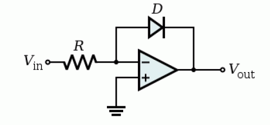
| This equation can also be used in order to make a basic Logarithmic Amplifier. The operational amplifier is taken as an ideal amplifier; hence we can use all the assumptions of an ideal operational amplifier. The assumption of virtual short is used here and the positive and negative ends of the OPAMP (2 and 3 pin are shorted) to ground. |
| The P-N junction diode is taken and used as a feedback loop of the operational amplifier (between 2 and 6 pin). The output voltage of the circuit (at pin 6) is the voltage across the diode as the voltage at pin 2 is 0v because of the virtual short concept.As the opamp consists of high input impedance so the current coming at pin 2 will go in the feedback loop instead of going inside opamp. |
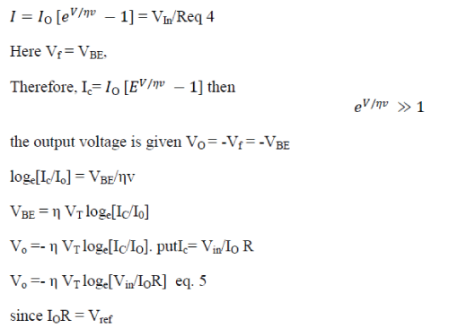
| Let the current flowing through the diode be If, current flowing through the resistor R be I1 and the voltage across the diode in the feedback be Vf.Therefore, we got I1 = If = Vin/R Substitute value in eq 2 |
| V = -η v [loge (If)- loge (Io)] (- sign because the n junction of the diode is at the same potential of the output VO) |
| V = -η v [loge (Vin/R)- loge (Io)] |
| V = -η v [loge (Vin/R Io)] eq 3 |
| Therefore from the above equation the result is that the output voltage is directly proportional to the logarithm of the input voltage. |
| To convert the form of the output in terms of log of base 10 then the following conversion is used the conversion factor calculated mathematically is 0.434. It means that if an attenuator with attenuation factor 0.434 is used before the logarithm amplifier then we can get the reading of the output as in the terms of log with base 10. The practical circuit mentioned is displayed below. This shows that using the log amplifier with base 10 will give less output in the comparison of using the log amplifiers with base e. |
I. Trans-Diode Amplifier:
|
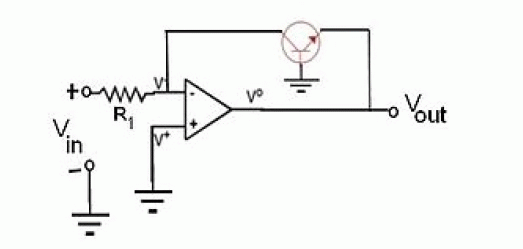
| Transistor can also act as a diode when connected in the common base configuration of the amplifiers. In the given figure it has been shown that the base is connected to ground also the collector is virtually connected to ground (as pin 2and 3 are connected to ground by virtual short concept). Here the collector and base are connected to ground, so they are shorted to each other. |
| Therefore the collector- base junction is short-circuited and transistor is equivalent to base-emitter junction which is equal to a diode as described in the following pair of equations. |
| Expression for output voltage: |
 |
| The output voltage of the trans-diode amplifier is proportional to the natural logarithm of input voltage, which is same for the diode in feedback amplifier. |
PROBLEMS WITH THE STABILITY
|
| There are various problems with trans-diode amplifiers such as: |
| A. The reverse saturation current is temperature dependent. Therefore with the change of ambient temperature there is a continuous change in the current which will change the output voltage. |
| B. There are also other temperature dependent term that is the VT, we have VT = T/1160. |
| C. There are also a lot of errors due to the input bias current, input offset voltage, input noise voltage. |
| However these type of errors can be reduced by the use of temperature compensation techniques and the by using of operational amplifiers with MOSFETS input voltage. |
| D. There are also some kinds of errors which arise due to the oscillations due to the presence of active gain element (transistor) in the feedback loop. |
| To overcome this problem there is a circuit which demolishes the oscillations by the introduction of a bypass capacitance and a feedback resistance. |
SOLUTIONS
|
| BARKHAUSEN’S CRITERION FOR OSCILLATIONS: |
| According to the Barkhausen’s criterion oscillations in any circuit can occur only and only if these two conditions are satisfied.The two conditions are: |
| A. The product of the gain of the circuit (amplifier) and the feedback factor should be equal to 1 that is A.β = 1. |
| B. The other condition is about the phase angle that is the total phase shift should be equal to 360o that is the total phase difference between the output and input is 360o. |
| In the trans-diode amplifier there are cases where the value of the product of the gain of the amplifier and the feedback factor is equal to 1. As in the case of transistor acting as a diode in the feedback will behave as a switch which will either give closed or open switch. The closed switch will give as gain as 1 (buffer amplifier), by this the condition of the product of gain and the feedback factor (which is generally 1) gives the output having the oscillations. |
| Also the second condition, about the total phase difference provided between the input and output is also satisfied by the trans-diode amplifier. As in this there is an operational amplifier which is provided with the input at the inverting terminal. Due to which a phase difference of 1800 is provided at the output with respect to the input of the amplifier. The other phase difference is provided by the means of the feedback, as there is a transistor in the feedback which is having the input at the collector and output connected to the emitter (also here the base is grounded, it is common base configuration). Since common base amplifier gives 1800 out of the phase output when an AC supply is provided to it atthe collector and the output is taken at the emitter. Therefore by the first case we have 1800 out of phase difference and by the second case we have the other 1800 out of phase difference, so in total we have the total phase difference as 3600 thus satisfying the second condition of Barkhausen’s Criterion. |
| Since both the conditions of Barkhausen’s Criterion are satisfied and the output of the trans-diode amplifier will give lot of oscillations. |
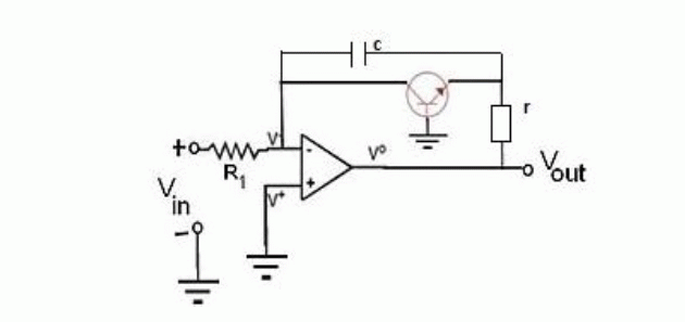
| To solve this problem a circuit is considered consisting of the trans-diode amplifier along with a resistor and a capacitor. The capacitor is attached in the parallel to the transistor and the resistance is added in the series with the transistor. |
| A. Purpose of capacitor: |
| The original use of capacitor in the field of electrical networks is as a charge storing device, the rate at which the charge stored is high and the rate of the charge dissipation is low means the charge will be stored in the capacitor when there is off state of transistor. |
| Generally the major role of capacitor in this circuit is to increase or decrease the total phase difference from input to the output. The capacitor will have a charge all the times, positive or negative depends on the input provided at the inverting terminal. According to the basic concept of the capacitor if a specific charge is present on one plate of the capacitor then the opposite charge will be present on theanother plate providing an additional phase shift of 1800. Due to this the total phase ship has change from 3600 to 3600+- phase shift provided by the capacitor (may be other than 1800). But as the total phase shift has changed from 3600 to something higher and lower, due to this the Barkhausen’s Criterion is not satisfied and the condition of oscillations is dismantled. |
| B. Purpose of Resistance: |
| In the above case the resistance is used as the feedback part. The resistance is generally a passive device used here in to order to change the feedback factor. The feedback factor in this case is related to the resistance connected in the emitter of the circuit as it is providing the negative feedback to the input. The current coming from the collector region to emitter region goes through the resistance therefore the output voltage is reduced due to the drop of voltage at the emitter resistance. |
| Generally in the common base configuration the feedback is due to the emitter resistance. The feedback factor β is inversely proportional to the resistance as mentioned above that this resistance is providing a negative feedback due to which |
| β = 1/Re |
| Since here the feedback factor is reduced due to presence of a resistance Re. In the above cases the feedback factor is generally 1 or infinite, now it is a finite quantity. Therefore the second condition of Barkhausen’s criterion is not satisfied, as the product of gain of the amplifier and feedback factor here is not 1. Therefore the condition is not satisfied. |
| By the above points it is cleared that by the introduction of these two extra components there is a decrease in the amount of oscillations. |
| In technical words the Re is called as emitter degeneration resistance which is used to reduce the feedback factor and the capacitor connected in the parallel of the transistor is the feedback capacitor which leads to feedback lead. |
PRACTICAL SIMULATIONS
|
| A practical experiment has been done in which the system is made to be implemented. The output is seen in the CRO. The circuit is also implemented on the PS-PICE and the simulation picture is shown in below. |
| This represents the simulation picture (figure 4) of the output with respect to time of a normal trans-diode amplifier in a ps-pice simulator. According to the simulation and the reading of the observationtable, it has been found that the oscillations are reduced a lot in the second circuit due to the capacitor and resistor. By the above readings and the simulation it has been cleared that by the means of additional circuit the oscillations are reduced and stability of the output is increased. |
CONCLUSION
|
| By the study of the provided the simulations and the practical readings, it is cleared that the role of feedback capacitor and the resistance have the large impact over the oscillations at the output of a normal trans-diode amplifier. It has been clearly seen that the oscillations are reduced in the circuit consisting with capacitors and feedback resistance |
ACKNOWLEDGEMENT
|
| The authors would like to thank all the people who helped him a lot at the time of collecting the data regarding this paper. The author would personally like to thank Prof. Vicky Chedda, Prof. Rupali Patil, Prof. HetalDoshi, Prof. SangeetaKulkarniand all other teachers who helped him for the simulation problems. Special thanks to Mstr. AmbrishChaturvedi, Mstr. Aditya Patil for their sincere help. |
Figures at a glance
|
 |
 |
 |
 |
| Figure 1 |
Figure 2 |
Figure 3 |
Figure 4 |
|
| |
References
|
- D. Johns and K. Martin, âÃâ¬Ãâ¢Analog Integrated CircuitDesign,âÃâ¬Ãâ John Wiley & Sons, 1997.
- M. Smith, âÃâ¬Ãâ¢A 0.5 to 4 GHz true logarithmic amplifier utilizing monolithicGaAs MESFET technology,âÃâ¬Ãâ IEEE Trans. Microwave TheoryTech., vol. 36, pp. 1986–1990, Dec. 1988.
- G. Acciari, F. Giannini, and E. Limiti, âÃâ¬Ãâ¢Theory and performance of parabolictrue logarithmic amplifier,âÃâ¬Ãâ Proc. IEE—Circuits Devices Syst.,vol.144, no. 4, pp. 223–228, Aug. 1997.
- 6. A. Garskamp, âÃâ¬Ãâ¢Logarithmic amplifier with sequentially limiting amplifierstages,âÃâ¬Ãâ U.S. Patent 5 049 829, Sept. 17, 1991.
- A. Woroncow and J. Croney, âÃâ¬Ãâ¢A true logarithmic amplifier usingtwin-gain stages,âÃâ¬Ãâ Radio Electron. Eng., pp. 149–155, Sept. 1966.
|