Keywords
|
| Boost Converter, Snubber cell, zero-current transition, zero-voltage transition. |
INTRODUCTION
|
| Switching frequency plays an important role in the operation of the converters. PWM dc–dc converters with high frequencies have been widely used in various power electronic applications such as power factor correction, battery charging, and renewable energy applications because of their high power density, fast transient response, and ease and simplicity in control. However, due to high-frequency operation switching losses occur, and has higher electromagnetic interference (EMI), and poor converter efficiency [1]. Switching losses and EMI noises of PWM converters are mainly generated during turn-on and turn-off switching transients [2]. |
| Conventional converters operate with hard switching or traditional switching and are known as hard switching converters. During turn ON period, the voltage across the switch tends to increase and the current tends to decrease, which results in some switching losses. Similarly during turn OFF period the voltage tends to increase and the current tends to decrease across the switch. Again it leads to some switching losses. Recently, switch-mode power supplies have become smaller and lighter due to higher switching frequency. However, higher switching frequency causes lots of periodic losses at turn ON and turn OFF, resulting in increasing losses of the whole system. Operating at high frequency with traditional hard switching pulse-width-modulation (PWM) converters is limited because of substantial switching loss. Again it leads to some switching losses that adversely affect the efficiency of operation. High switching losses furthermost reduce the power-handling capabilities of the converters hence reducing their life span and causing limited efficiency. Also transition intervals take long time and cause conduction losses over one switching cycle [3]. |
| In the conventional ZCT-PWM converter or ‘hard switched’ PWM converters [4], the main switch turns OFF with ZCS and ZVS. The auxiliary switch turns ON with near ZCS. The operation of the circuit is mainly dependant on load conditions of the converter. When the main switch turns ON, reverse recovery current of the diode flows across the main diode and results in the occurrence of a short circuit between the main switch and the diode. The auxiliary switch turns OFF by hard switching and their parasitic capacitors discharge through the switches [3], [10] [7]. In the conventional zero-voltage transition (ZVT)-PWM converter [2], the main switch turns ON with ZVT perfectly by means of a snubber cell. And also the main switch turns OFF under near zero voltage switching (ZVS). The main diode turns ON and OFF under ZVS. The auxiliary switch turns ON with near zero-current switching (ZCS) and turns OFF with traditional hard switching process. The operating frequency of the converter defines its size and cost. In order to find a better solution to the problem of ZVT and ZCT converters, many ZVT–ZCT–PWM dc–dc converters are proposed that combines the ZVT and ZCT ideas that are suggested in the research works done in [9], [15], [16]. In these types of converters, the main switch turns ON and turns OFF with zero voltage and zero current, respectively. But the auxiliary switch is turned ON and turned OFF by soft switching method. Further in [9], the main switch turns OFF and turns ON with ZCS and ZVS. And also the main diode turns ON and turns OFF with ZVS.The drawbacks of the converter are the input voltage must be smaller than half of the output voltage for soft-switching operation, there is a presence of additional current stress on the switches, switching intervals taking long time and cause conduction losses over one switching cycle. In [15], the main switch turns ON with zero voltage transition and turns OFF with zero current transition. It does not have any additional voltage and current stresses on the main switch and the main diode. Also with further advances in the field, a magnetic coupled inductance is used in the circuit which adds to the complexity of the circuit. And when the magnetic coupling is not proper, parasitic oscillations takes place and losses occur due to the presence of leakage inductance. The turn off of the auxiliary switch by soft switching method and the transfer of the energy stored in the inductor are very difficult in converter circuit and require additional auxiliary circuits to accomplish the process. |
| Furthermost the design of EMI filter and control circuit topology is complicated and very hard to be optimized and analyzed. Conduction losses will subsequently increase due to higher circulating current involved [10].Therefore many solutions have been proposed to minimize the switching losses of the converter and up to date, a number of softswitching technologies have been proposed to reduce switching loss but only at the cost of sacrificing the efficiency and compromising with the performance of PWM converters. |
| A lot of work has been carried out in this regard and number of papers is submitted so as to solve the problems of the conventional converter circuits [2], [3], [5], [8]. But the main disadvantage is the increase in voltage and current stress across the circuit components and reduced efficiency. In order to overcome these above mentioned problems, a new ZVT-ZCT-PWM dc-dc converter that combines ZVT-ZCT methods are also suggested [7], [9], and [10]. Various advancements in semiconductor technologies to produce high power devices have facilitated numerous applications where high power density is very important for practical and sophisticated solutions. In these converters, the turn on or off process takes place under ZVS and/or ZCS during a very short period of Zero Voltage Transition (ZVT) or ZCT time provided by a resonance. Hence, the resonant converters are used to operate at higher switching frequencies. Most of the new soft-switching converters reduce switching loss only at the expense of much increased voltage/current stresses of the switches, which leads to a substantial increase in conduction loss. |
| Therefore, this problem of switching gave raise to further research works. When studied these above mentioned parameters in detail, it was analysed that there is a possibility of improving the operational range and efficiency of the converter. And it was found that there was a good scope for overcoming these hazardous phenomena by proposing few changes in control strategies and operating topologies. Hence this gave an important turn-over in the field of power electronics But the best solution for this problem is found to be the use of a new active snubber cell for the boost converter has been designed in this proposal which operates at soft switching even at higher switching frequencies and performance can be enhanced by operating them at high frequency levels incorporated with soft switching (SS) techniques [1] by implementing snubber to them. |
| An extensive literature survey and the study about the present topologies concluded the need of a converter which has the advantages of both ZVS and ZCS technique and to eliminate the disadvantages of conventional converters a better option is to have a converter with both ZVS and ZCS, where a transition period is created for switching on and off the switches. Resonant converters are a family of soft-switching converters in which a resonant tank is added to the converter that reduces switching losses significantly by means of the commutations which are realized with either zero voltage switching (ZVS) or zero current switching (ZCS). Resonant converters have high efficiency, small size, light weight, fast dynamic response, low component stresses and low noise. Applications of such ZVT-ZCT PWM DC-DC converter are suitable for the power-factor correction circuits and the renewable energy converters, where high efficiency is considered mainly [1]. |
| This Soft switching (SS) technique allows operation of the proposed converter at higher switching frequencies resulting in higher power densities without compromising the efficiency. Switches have to provide a reverse voltage blocking capability and for this reason they have to be constructed by means of an IGBT or a MOSFET having a reverse voltage blocking diode with them. Snubbers can control the voltage and current to a point where switching occurs at zero voltage and zero current and thus increases the reliability of the power stage significantly. In the proposed work, size and weight of the device is reduced as the heat sink is not required. |
| There are three approaches to have the high efficiency in the proposed converter- |
| • During the control range of operation, the transistor current and voltage waveforms does not overlap with each other due to which the power dissipation of the circuit is reduced. |
| • In this converter all the semiconductor devices operate under soft switching, hence switching losses are totally eliminated. |
| • There is negligible circulating current from the auxiliary circuit to the main switch so that the main switch maximum current and conduction losses are not increased. |
SYSTEM MODEL AND ASSUMPTIONS
|
| The following assumptions are made for the converter analysis: |
| 1. Input voltage is constant. |
| 2. Main inductor is much greater than resonant inductor. |
| 3. The output capacitor is large enough to assume that the output voltage is constant and ripple free. |
| 4. Resonant circuits are ideal. |
| The circuit presented in this study is a new active snubber cell that turns ON and turns OFF by exactly ZVT and ZCT respectively and is developed without any considerable increase in the cost and the complexity of the converter. This is called a new ZVT-ZCT PWM converter shown in Fig. 1. In the circuit proposed, input voltage source is , is the main inductor, and is the output capacitor which acts as a filter capacitor. S1 is a main switch which consists of a main transistor T1 and has a body diode D1. The snubber circuit is formed by snubber inductor Ls, a snubber capacitor Cs and auxiliary switch S2 that has a auxiliary transistor T2 and D2is its body diode respectively and the diodes are bypass diodes which prevents the additional stress on the auxiliary switch. This work presents an efficient resonant boost converter topology for soft switching technique with an active snubber cell. It first presents the analysis of the system operation that is supported by a mathematical description and also it provides the simulation results using MATLAB-Simulink platform. |
| As shown in the circuit, is the main switch that is constructed by means of IGBT and is the auxiliary switch made up of MOSFET. Initially and are in off condition. is the input current flowing through main diode . The voltage across snubber capacitor is dependent on efficiency of the resonant circuit. When turn ON signal is applied to the gate of , a resonance starts developing between and due to which current increases and current falls. Rate of rise of current is governed by connected in series to . Hence turns ON with ZCS which defines soft switching (SS). Meanwhile is charged to a particular value. Due to this falls to zero and becomes negative in order to turn OFF . Now is ON and conducts input current. At this stage a new resonance between and starts. is a parasitic capacitor which is assumed to be sum of capacitances of switch [1]. When becomes zero, the energy stored in it is further transferred to the resonant circuit for its operation. Now turns ON with nearly ZVS condition. Resonance between the snubber components continues for further also. This shows the ZVT duration of the main switch. Hence is turned OFF with ZCT without any additional current stress on it. Diode becomes ON. Snubber circuit does not work when current through snubber inductor reaches zero and hence it is similar to ON stage of the conventional boost converter where snubber is inactive. |
| Then a control signal when applied to a new resonance starts and it is turned ON with ZCS. turns OFF with ZVS and ZCS. A resonance starts between , , of the resonant circuit. The control signal of is removed, is charged linearly to input voltage and main diode is turned OFF under ZVS. This is similar to OFF mode of the conventional boost converter in which snubber is inactive. This above explanation completes one switching cycle. |
DESIGN CONSIDERATIONS
|
| The main calculation in the system design includes the calculation of the snubber components along with the load parameters. |
| 1. Resonant capacitor Cr |
| The resonant capacitor Cr is the sum of the parasitic capacitor of S1 and the other parasitic capacitors incorporating it. The value of Cr is approximately 1nF. |
| 2. Snubber inductor Ls |
| To turn ON auxiliary switch with ZCS, the required series inductor Ls is calculated |
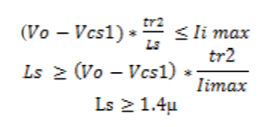 |
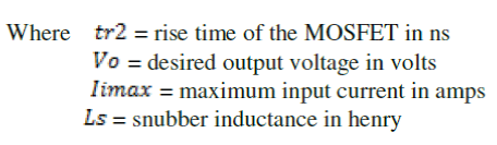 |
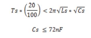
| 3. Snubber capacitor Cs |
| The resonant capacitor is calculated depending on the transient intervals. The sum of the transient intervals is selected to be less than 20% of the switching period. |
 |
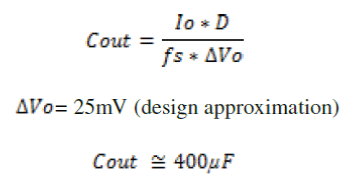
| 4. Output filter capacitor Cf |
| Cf is an output filter capacitor and is used to filter out the ripples and harmonics in the converter operation. |
 |
| The proposed circuit is designed for 1kw and 1000kHz with a duty cycle of 60% for the main switch. |
| From the above designed parameters the proposed circuit is simulated in MATLAB Simulink software package and hence appropriate results are obtained as shown below. The overall efficiency of 98% is obtained. The obtained values can be considered as the first approximations, which can be verified further in the next section. |
SIMULATION RESULTS AND DISCUSSIONS
|
| This section provides the simulation results for the proposed circuit. It provides soft switching methodology and thus the transistors are switched ON and OFF under ZVS and ZCS respectively. The converter output current is sinusoidal in shape. |
| The Fig. 2 shows the Simulink model for the proposed converter configuration. The circuit is built using MATLAB simulation package with an input voltage of 200V, a switching frequency of 100 KHz and duty cycle of 60%. This waveform shown in Fig. 3 is the voltage across the main switch. IGBT is used as the primary switch in the circuit. |
| Since IGBT is designed to turn on and off rapidly, a constant pulse waveform can be observed across the switch whose voltage is equal to the output voltage of the converter. High current, high voltage and higher switching frequencies favour IGBT operation. |
| The Fig. 4 shows the current through the main switch of the converter. Since IGBT is a minority charge carrier device, it has high current carrying capability. This property is useful in higher frequency operations where the large currents have to be utilized. The technique of soft switching is applicable to fast IGBT with a relatively small current tail. However, employing ZCS technique eliminates the voltage and current overlap by forcing the switch current to zero before the switch voltage rises. |
| The Fig. 5 shows the current flowing through the auxiliary switch of the converter. MOSFET along with its body diode is used as auxiliary switch in the proposed work. The voltage is a pulse wave that is obtained by soft switching of the converter. The auxiliary switch is in parallel to dc input voltage source. Near zero-voltage turn-on condition is created by a current injection from the auxiliary branch that contains a resonant inductor, an auxiliary switch, and snubber capacitors. The main switch is turned on while the voltage across the main switch drops nearly to zero after resonance. |
| Soft-switching conditions are maintained at very wide line and load ranges. Also, the voltage and current stresses on the auxiliary components stay at allowable levels. Thus, an auxiliary switch with smaller parasitic capacitance can be utilized and turn-on loss of the auxiliary switch is smaller as shown in Fig. 6 |
| The Fig. 7 shows the voltage across the snubber capacitor. Snubber capacitor or resonant capacitor plays a vital role in the converter operation by charging up the output voltage. Snubber capacitor is selected to charge up to approximately the output voltage, when the energy accumulated in the snubber inductor is transferred completely to it. |
| The output capacitor is large enough so that the output voltage is maintained at constant level and is ripple free. The ZCT duration tends to increase when Cs and Ls increases as shown as in Fig. 8. The ZCT duration depends on the resonance between Ls and Cs. Consequently, because the resonances occur during very short time periods during the operation, the converter acts as a normal PWM converter during most of the time which is an added advantage of the circuit. |
| The occurrence of the ZVT and ZCT is the main concentration in the proposed converter circuit. The Fig. 9 shows this evidently. Soft switching can apply to semiconductor devices in not only the original converters, but also the snubber cells. |
| These IGBT and MOSFET devices which play a vital role in power electronics field are used in many HVDC applications due to high efficiency, fast switching, low conduction voltage drop, and high current carrying capability. IGBT is the device of choice when high current and high voltage application is considered because of its easily driven MOS gate. Due to the elimination of the switching losses by soft switching, the efficiency is comparatively higher than the conventional circuit. From the voltage, current, and control waveforms of the main switch S1, given in Fig. 3, it can be seen that S1 is operated perfectly under soft switching condition at both turn ON and turn OFF processes. There is no overlap between voltage and current waveforms of the main switch. Fig. 9 Shows ZVT-ZCT realization for the main switch by which it is clear that the proposed circuit overcomes the demerits of conventional one. The overall efficiency of the proposed converter is measured to be 98% at the nominal output power. |
EFFICIENCY DISCUSSION
|
| The Fig. 10 shows the efficiency graph for the proposed novel ZVT-ZCT Boost converter. The graph explains about the varying efficiency for varying output power. The graph is plotted with efficiency of the converter (%) in x-axis versus the output power of the converter (watts) at y-axis. In the conventional converters the efficiency is limited when operated at higher frequencies and when the frequency increases, the waveform becomes distorted. Hence, when this condition is analysed and a convincing result is obtained by performing the simulations for calculated parameter variations for the proposed circuit configuration by considering the output power of various values, it can be seen that the efficiency of the converter increases substantially with the parameters that are considered. From the graph it can be concluded that maximum efficiency is obtained when power output approximately nearer to 1Kw is used for the designed converter. And also, it can be seen that the efficiency values of the proposed converter are much higher than that of the hard switching converter. The efficiency obtained at a constant frequency of 100 kHz is determined to be more than 98%. This shows that efficiency of the converter can be substantially increased by operating at higher frequencies without having switching losses. Since the converter design is simpler with minimum number of components, this topology can be easily applied to the other PWM converters. |
CONCLUSION
|
| In this paper, a new active snubber cell is proposed that provides ZVT and ZCT while turn on and turn off of the main switch respectively. To completely eliminate switching losses and EMI noises, soft switching is applied to all the semiconductor devices of the proposed one. Any additional current and voltage stress does not occur on the switches. Moreover the converter has a simple structure, ease of control and low cost. Hence the snubber cell can easily be applied to other PWM converters. The proposed work was designed at 1Kw and 100 kHz with a duty cycle of 60% and a desirable efficiency of 98% is achieved which increases reliability of the converter. The proposed converter combines the advantageous features of conventional converter to develop in to a ZVT-ZCT converter. The circulating energy is quite small and can be neglected. Also the converter can operate at higher frequencies that can be useful in various industrial applications. |
Figures at a glance
|
 |
 |
 |
 |
 |
| Figure 1 |
Figure 2 |
Figure 3 |
Figure 4 |
Figure 5 |
 |
 |
 |
 |
 |
| Figure 6 |
Figure 7 |
Figure 8 |
Figure 9 |
Figure 10 |
|
| |
References
|
- NihanAltintas¸, A. FarukBakan, and Ismail Aksoy “A Novel ZVT-ZCT-PWM Boost Converter” IEEE transactions on power electronics, vol.29, no. 1, January 2014.
- C. J. Tseng and C. L. Chen, “Novel ZVT-PWM converters with active Snubbers,” IEEE Trans. Power Electron., vol. 13, no. 5, pp. 861–869,Sep. 1998
- G.Hua, E. X.Yang,Y. Jiang, and F. C. Lee, “Novel zero-current-transition PWM converters,” IEEE Trans. Power Electron., vol. 9, pp. 601–606, Nov. 1994.
- G. Hua, C. S. Leu, Y. Jiang, and F. C. Lee, “Novel zero-voltage-transition PWM converters,” IEEE Trans. Power Electron., vol. 9, no. 2, pp.213– 219, Mar. 1994.
- J. G. Cho, J. W. Baek, G. H. Rim, and I. Kang, “Novel zero-voltage transition PWM multiphase converters,” IEEE Trans. Power Electron., vol.13, no. 1, pp. 152–159, Jan. 1998.
- J. M. P. Menegaz, M. A. Co., D. S. L. Simonetti, and L. F. Vieira, “Improving the operation of ZVT DC-DC Converters,” in Proc. 30th PowerElectron. Spec. Conf., 1999, vol. 1, pp. 293–297.
- I. Aksoy, H. Bodur, and A. F. Bakan, “A new ZVT-ZCT-PWM DC–DC converter,” IEEE Trans. Power Electron., vol. 25, no. 8, pp. 2093–2105, Aug. 2010.
- W. Huang and G. Moschopoulos, “A new family of zero-voltage-transition PWM converters with dual active auxiliary circuits,” IEEE Trans.Power Electron., vol. 21, no. 2, pp. 370–379, Mar. 2006.
- H. Bodur and A. F. Bakan, “A new ZVT-ZCT-PWM DC-DC converter,” IEEE Trans. Power Electron., vol. 19, no. 3, pp. 676–684, May 2004.
- H. Bodur and A. F. Bakan, “A new ZVT-PWM DC-DC converter,” IEEE Trans. Power Electron., vol. 17, no. 1, pp. 40–47, Jan. 2002.
- H. Wannian, G. Xing, S. Bassan, and G. Moschopoulos, “Novel dual auxiliary circuits for ZVT-PWM converters,” Can. J. Electra. Compute.Eng., vol.33, pp. 153–160, Summer-Fall 2008.
- D. Y. Lee, B. K. Lee, S. B. Yoo, and D. S. Hyun, “An improved full bridge zero-voltage-transition PWM DC/DC converter with zero-voltage /zero-current switching of the auxiliary switches,” IEEE Trans. Ind. Appl., vol. 36, no. 2, pp. 558–566, Mar./Apr. 2000.
- C. M. de O. Stein and H. L. Hey, “A true ZCZVT commutation cell for PWM converters,” IEEE Trans. Power Electron., vol. 15, no. 1, pp.185– 193, Jan. 2000.
- H. Mao, F. C. Lee, X. Zhou, H. Dai, M. Cosan, and D. Boroyevich, “Improved zero-current-transition converters for high-power applications,” IEEE Trans. Ind. Appl., vol. 33, no. 5, pp. 1220–1232, Sep./Oct. 1997.
- D. Y. Lee, M. K. Lee, D. S. Hyun, and I. Choy, “New zero-current transition PWM DC/DC converters without current stress,” IEEE Trans.Power Electron., vol. 18, no. 1, pp. 95–104, Jan. 2003.
|