International Journal of Innovative Research in Science, Engineering and Technology
ISSN ONLINE(2319-8753)PRINT(2347-6710)
ISSN ONLINE(2319-8753)PRINT(2347-6710)
Madhumita Singh1, Sanjeev M. Ranjan2, Zoonubiya Ali3
|
| Related article at Pubmed, Scholar Google |
Visit for more related articles at International Journal of Innovative Research in Science, Engineering and Technology
Voltage controlled oscillators are critical block in analog circuit. It is integral part of phase locked loop, clock and data recovery circuit and frequency synthesizer. This paper presents review of different oscillator structure used in various applications. Also this paper proposes a new oscillator design which has high tuning range and less chip area.
Keywords |
| Oscillator, phase locked loop, clock and data recovery circuit, frequency synthesizer. |
INTRODUCTION |
| A signal generating circuit is one of the most important building blocks in analog, digital and mixed-signal designs. Oscillators play a critical role in communication systems, providing periodic signals required for timing in digital circuits and frequency translation in radio frequency (RF) circuits. The most popular oscillator architecture for RF applications is mainly either a LC oscillator or a ring oscillator. The basic circuit of LC oscillators is presented in [1]. To improve the circuit performance many circuits were proposed. To compensate the tank losses of LC oscillator cross coupled oscillator is used [2]. As compared to this cross coupled circuit complementary cross coupled circuit gives large number of advantages [3]. As the requirement of quadrature signal in communication system quadrature VCO is presented [1]. Ring oscillator basic circuit is presented in [4] which comprises of inverting stage and delay stage. Numerous type of these two stages are presented in [4], [5], [6], [7].Oscillator based on band pass filter [8], active inductor [9] etc. is also used to meet the applications requirements. |
| A LC oscillator exhibits good phase noise, but a fabrication cost is expensive due to an inductor and it consumes a large chip area. A narrow frequency tuning range is another downside of a LC oscillator. A ring oscillator can be built in a standard CMOS process with a small silicon area, and a frequency tuning range is very wide compared with a LC oscillator. However, a ring oscillator has poor phase noise performance and it is sensitive to a power supply induced noise. |
| This paper presents a new oscillator design which is based on band pass filter using active inductors. This oscillator improves phase noise performance and has wide tuning range. |
OSCILLATOR |
| An oscillator is an amplifier which uses a positive feedback and without any external input signal, generates an output frequency at a desired frequency. It converts DC power (from the supply) to a periodic signal. |
| A. Types of oscillators |
| Voltage controlled oscillators can be categorized by method of oscillation into resonator-based oscillators and waveform-based oscillators. Resonator based oscillators are categorized into LC and Crystal oscillator. And waveform based oscillator divided into Relaxation and Ring oscillator. Each type has different ways of doing frequency tuning such as current steering for ring oscillator and variable capacitor for LC oscillators. Ring and LC oscillators are good choice for different application. Relaxation and crystal oscillator are not a good choice due to huge phase noise and impractical to design, respectively. |
| 1) LC Oscillator. |
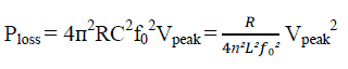
| A general LC VCO is shown in fig. 1(a) in which inductance L and capacitance C consist of a parallel resonance tank and RL and RC are the parasitic resistance of the inductance and the capacitance, respectively. A negative resistance –R is used to realize in order compensate the losses coming from RL, RC and active component like CMOS transistors. The loss in the tank can be expressed as [1]: |
 (1) (1) |
| Where R represents the combined losses of the inductance and the capacitance, and Vpeak is the peak voltage amplitude across the capacitance. It can be observed from (1) that the power loss decreases linearly with the series resistance in the resonance tank, and it also decreases quadratically with an increase of the tank inductance. |
 |
| 2) Cross Coupled Oscillator |
| To compensate the losses in resonant tank from both parasitic resistance and capacitance, a negative resistance –R is formed in tank. But in real there is no existence of negative resistance it is formed by cross coupling transistors as shown in fig 1(b). By cross connecting the output to the oscillator, negative resistance that has the same conductance as the transistor’s transconductance (gm) is created. The phase noise of LC VCO is inversely proportional to the quality factor (Q2) [2]. So if we increase quality factor of the LC tank, the phase noise will be improved. The quality factor of LC tank can be expressed as |
| Where Gtot is the transconductance of the LC tank and Gtot can be expressed as |
| Gtot = Gp - Gn (3) |
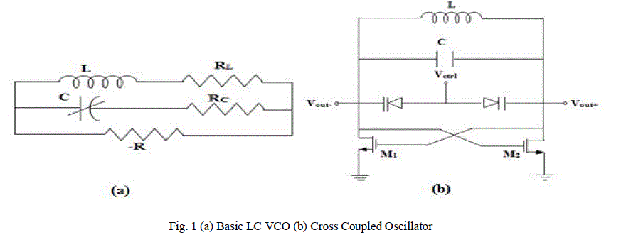
| Where Gn added negative conductance to the circuit that can decreases Gtot and therefore, quality factor increases which improve phase noise of circuit. To improve power consumption as well as phase noise differential cross coupled oscillator with decoupled capacitor and polysilicon resistor is used as shown in fig 2(a). |
| 3) Complimentary Cross Coupled Oscillator |
| A fully integrated complementary cross-coupled configuration as shown in fig 2(b) is chosen because of the following advantages [3]. |
| a) The complementary structure offers higher transconductance at a given current, which results in faster switching of a cross-coupled differential pair. |
| b) It performs better rise- and fall-time symmetry, which results in less upconversion 1⁄f of noise with the other low-frequency noise sources. |
| c) The dc voltage dropping across the channel is larger for the all-NMOS structure since the dc value of the drain voltage is Vdd. There is, therefore, stronger velocity saturation and a larger γ. |
| The active devices (NMOS1, NMOS2, PMOS1 and PMOS2) serve as negative resistor to compensate LC tank losses. The cross coupled VCO operates as switches. Oscillator forces VGD of NMOS transistor to generate the differential voltage across the resonator. At the differential zero voltage all four switching transistor are in saturation region and form small- signal negative conductance which start the oscillation. As the differential oscillation voltage crosses Vth,n, |
 |
| VGD of NMOS1 exceeds +Vth,n, forcing it into the triode region, VGD of NMOS2 falls below +Vth,n, driving the device into a deeper saturation region, and then NMOS2 turns off. |
| Simultaneously, as the falling differential oscillation voltage crosses - Vth,p, VDG of PMOS1 exceeds –Vth,p , forcing it into the triode region, at the same time, VDG of PMOS1 forces itself into deeper saturation, and then PMOS1 turns off. Thus, the complementary LC tank VCO operates when both NMOS and PMOS pairs are all in the saturation region beforehand, then NMOS1 and PMOS2 are at the off states, while other NMOS2 and PMOS1 are at the on states. Such a switching process is periodical throughout the operation of the VCO. The current Ibias, drives the LC tank VCO into the stable operation. |
| 4) Quadrature VCO. |
| Different design options are available to generate quadrature signals. Some are discussed here: |
| a) Combination of VCO, polyphase- filter (or R-C, C-R filter), and output buffers (or limiter) are used. [10], [11]. It consists of four output buffers or limiters. If buffer are inserted between VCO and filter, more power is needed; if the filter is directly connected to the VCO, tank capacitance is increased, leading to the higher power consumption and worse phase noise. Furthermore, a lot of chip area is needed, as the filters need good matching. |
| b) VCO at double frequency followed by master- slave flipflops. It needs a VCO designed at double frequency, which should not consume more power, as a higher QPS for integrated tanks at higher frequencies is achievable (Inductance scales down linearly when sizing down an integrated coil, coil capacitance scales down quadratically, so L/C improves). Master- slave flip flops in this consumes too much of power. |
| c) Two cross coupled VCO’s [12]. It consumes less power consumption as compared to above two options. It provides a very high voltage swing which eases the design of prescaler and mixer circuits connected to the VCO. This consideration can also be extended to VCO’s using external high- quality inductors. When using external inductors, a lot of current must be spent to amplify the VCO signal to drive the Polyphase filters or to drive the flipflop. |
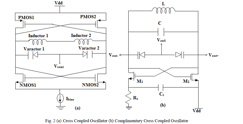
| d) Current reusing topology. The combination of NMOS and PMOS transistors are used to realize the negative resistance [13] was chosen as it reuses the dc current. Furthermore, the current source was omitted to maximize the signal swing as shown in fig 3. [1]. Omiting current source has few more advantages. It eliminates phase noise source. As all VCO- core transistors are put in a gigahertz- switching bias condition, flicker noise terms apparently are reduced by about 10 dB comparing measurement and simulation for several measured designs using this topology. The |
 |
| main disadvantage of omitting the current source is the increased sensitivity to the power supply. This effect can be reduced by the integration of a voltage regulator Other possible disadvantages of this are the increased spectral impurity of the oscillator signal and the less symmetrical waveforms, resulting in an increased up conversion of flicker noise. Both effects can be damped by the band pass characteristic of a well designed resonance tank. This topology guarantees to limit all gate voltages to the supply voltage. |
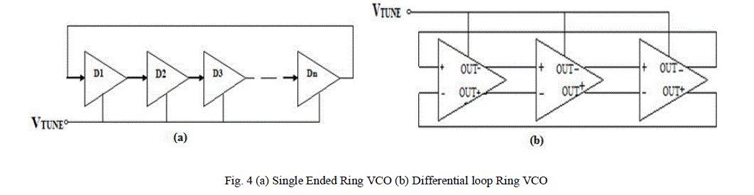
| 5) Ring Oscillator |
| A ring oscillator is comprised of a number of delay stages, with the output of the last stage fed back to the input of the first. To achieve oscillation, the ring must provide a phase shift of 2п and have unity voltage gain at the oscillation frequency. Each delay stage must provide a phase shift of п/N, where n is the number of delay stages. The remaining phase shift is provided by a dc inversion. Ring oscillator has two types as: [4] |
| a) Single Ended Ring Oscillator: D1 to Dn represent the delay cells, which provide the gain and the phase shift. They construct a closed loop by cascading all stages as shown in fig 4 (a). An odd number of stages are necessary for the dc inversion. |
| b) Differential loop Ring VCO: The differential ring oscillator is widely used, since it has a differential output to reject common-mode noise, power supply noise and so on. Fig.4 (b), depicts N stage ring oscillator realized using differential cells (which have complementary output).A source coupled pair (SCL) inverter will be a typical implementation. Assume that at time t0 the output of stage 1 changes to logic 1.When this logic 1 propagates to the end, it creates a logic 1 at the Nth stage, which, when feedback to the input of the first stage, creates a logic 0 in the first stage output. When this logic 0 is propagating through the chain, it toggles the output of stage 1 trigger next stage. It takes two passes through the chain to complete a period. Denoting tp as the propagation delay through each stage, then period T=2Ntp. For a differential cell N can be odd/even, to start an oscillation. |
 |
| 6) Ring inverting stage |
| There are numerous types of inverter stages by which a ring oscillator can be realized [13]. Some of the standard solutions are pictured in fig 5. [5], [6]. |
| Design in fig 5 (b) (c) (d) are of current starved type, for which the charging and discharging output capacitor current is limited by a bias circuit. The basic type and current starved with symmetrical load inverters have the highest, while current starved with output switching inverter has the lowest sensitivity. The ratio of relative frequency deviations between basic type and current starved with output switching inverter is 5:1. In general frequency deviation of all is same. Several typical design solutions with reduced sensitivity are also available known as combined ring |
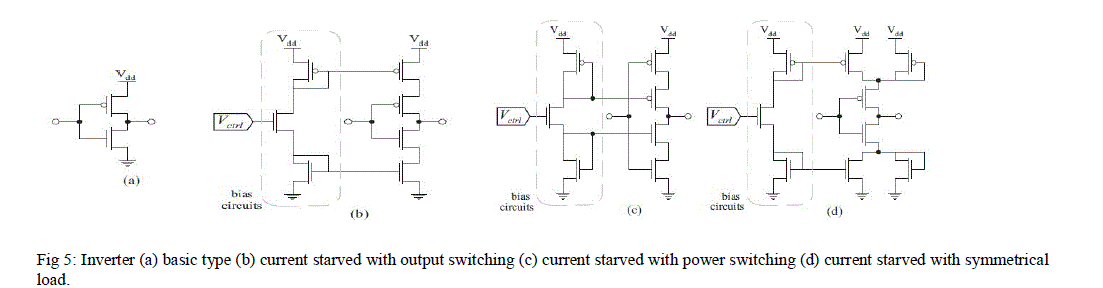 |
| current oscillator. In this the odd number inverter stages are implemented with basic type, while even numbered as starved with output- switching inverters. |
| 7) Differential delay cell |
| There are many features that differentiate the delay cell used in ring oscillator. Delay cell are categorized into three types on the basis of slew time which determines the overall phase noise [4]. |
| First is fast-slewing saturated delay cell. This delay cell has fast rise and fall time. It also performs full switching and therefore belongs to the saturated class of delay cell. |
| The second type of delay cell is a slow slewing saturated delay cell. Here the inverter consists of a source of a source coupled pair (SCP) and hence this is a current based inverter. It is called slow slewing because it has a longer gate delay. |
| The third type of delay cell is non saturated delay cell. This is also a voltage inverter based delay cell. In this delay cell some transistors are never on/off as a result output waveform never reach Vdd or ground, which is why this type of delay cell is called nonsaturated. |
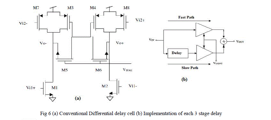
| Delay cell in differential ring oscillator are also used to reduce the phase noise. Delay cell employs differential pair as input and uses various types of load to get enough gain. Schematic of conventional delay cell [7] is shown in fig 6(a). In this circuit, NMOS transistors M1 and M2 form the primary loop, while the PMOS transistors M7 and M8 form the secondary loop. The primary inputs are fed from the outputs of the previous stage. The secondary inputs are fed from the outputs that are a few stages prior to the current stage. Output nodes will be precharged from M7 or M8. As a result, the output node can charge to a high voltage faster and hence increases the oscillation frequency. The PMOS load transistors M3 and M4 constitutes a latch. The strength of the latch also affects the oscillation frequency. The output oscillates from rail to rail because of latch and therefore, on- time of the transistors in the delay cell is reduced which further reduces the phase noise. The control voltage Vc at the gate of NMOS transistors M5 and M6 control the feedback strength of the latch. As Vtune is increased, the latch becomes strong and hence resists the voltage switching in the delay cell. It increases the delay time of the differential delay cell and reduces the oscillation frequency. The tuning voltage range of this conventional delay cell is limited. |
| Another method is delay interpolation. As shown in fig 6(b), each stage consists of a fast and a slow path whose outputs are summed together. By steering the current between the fast and the slow paths, the amount of delay achieved through each stage and hence the VCO frequency can be adjusted. |
 |
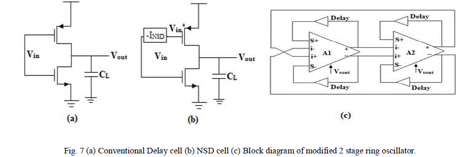
| 8) Negative Skewed Delay Cell |
| Negative skewed delay scheme is used to improve the operating speed of ring oscillator. Fig 7(b) shows the concept of negative skewed delay. Both the p- MOSFET and n-MOSFET have the same input in the conventional delay circuit as shown in fig 7(a), but in the negative skewed scheme, the p- MOSFET is connected to a negative delay element so that the input signal to the p- MOSFET arrives earlier than that to the n- MOSFET. Modified version of the delay cell as shown in fig 7 (c) is used to increase the tuning range and maximum operating range of ring oscillator at the cost of more power consumption. It consists of a conventional CMOS inverter and a conceptual negative delay element inserted at one of the two transistor inputs of the CMOS inverter. In this case, the input of the PMOS is connected to the negative delay elements and the input signal to the PMOS comes earlier than that of the NMOS. This features a self skewing local action per stage. This lead to a significant improvement in speed up to 3 times faster than conventional one. |
| 9) Based on active inductor |
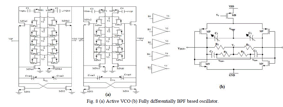
| Most of communication systems require a quadrature signal generator. Therefore it is necessary to construct a programmable wideband QVCO for modern multi-band transceivers. The popular method to generate quadrature signal is coupling two VCO cores either in series or parallel ways. However, additional transistors for coupling can either deteriorate the phase-noise performance of the circuit or limit the frequency tuning range. A new coupling method for the QVCO using active inductors is presented. In fig 8 (a), capacitors C1–4 connect the output nodes of one VCO core to the upper current sources of the active inductors in the other VCO core. The presented QVCO also has five frequency tuning bands which are the same as those of the single VCO. Though the QVCO can also achieve continuous wide frequency tuning, the oscillation frequency and tuning range of the QVCO may shift a little from those of the VCO due to the injection-locking phenomenon. |
| 10) Band pass filter based oscillator |
| A conventional BPF-based oscillator is a Wien-bridge oscillator. Fig. 8 (b) depicts a transistor-level schematic of the fully differential oscillator. R1, R2, C1 and C2 form a BPF, and transistors MN and MP take the voltage at the output of the BPF (V+ BPF and VBPF) and transform these voltages to currents which are fed back to the BPF. For positive feedback, a fully differential circuit is used. The oscillator output is taken from V+ OUT and VOUT as they have larger amplitude than the BPF output (V+ BPF and VBPF). Transistor MB is used to bias MN and MP and also provides a shielding effect from power supply noise. The common-mode voltage of V+ OUT and VOUT is sensed by R1, and is used to bias the gate voltages of MN and MP through R2. Once gm of MN and MP are set larger than the minimum requirement given by (5), then the oscillation starts and the oscillation frequency is fixed at ω0 as described in (5). The open loop transfer function of the BPF yields |
 (4) (4) |
 |
| The oscillation frequency that is set by the BPF center frequency ω0, and the minimum requirement for gm are given by |
 (5)&(6) (5)&(6) |
| The power supply noise sensitivity is improved over ring oscillator and has a wider ω0 tuning range than LC oscillator. In this oscillator R and C both are adjusted for tuning. And also consume less chip area than LC and ring oscillator both. Due to the low Q factor of the BPF based oscillator, its phase noise is worse than an LC oscillator but comparable to a ring oscillator. |
PROPOSED RF OSCILLATOR DESIGN |
| It consists of band pass filter with active inductor as shown in fig 9. M3 and M4 are employed for the input buffer stage. They are large devices and biased to have low input impedance and small distortion. A pair of PMOS active inductors M1a (or b) and M2a (or b) are employed to fulfill the frequency selectivity of the filter. PMOS are chosen mainly for two reasons: |
| a) The unity gain frequency of PMOS is tuned high enough to cover the filter frequency. |
| b) It is convenient to reuse the biasing currents of other stages, which are made of NMOS transistors. |
| The biasing current of input stage is reused by M1a and M1b. The gate voltage of M2a and M2b is tunable externally. The NIC (negative impedance circuit) can be realized by cross coupled differential pair to enhance the Q by compensating the active inductor noise. Multi tanh circuit structure is used as the negative transconductance stage. It is composed of a cross connected differential pair Mn1,2 and two unbalanced pair Mn 3,4 and Mn 5,6 with the size ratio of 4 to 1. When the signal is large enough that the symmetrical differential pair has saturated, the unbalanced differential pair can still provide the differential current proportional to the input voltage. Output buffer stage M5 and M6 is designed as common source stage which has high linearity. Fc is increased by increasing the bias current Ib of the active inductors. It is also increased due to the current reused by the active inductors. Q can be tuned by increasing NIC’s biasing current Iq. Transistor MN and MP take the voltage at the output of the BPF [V+ BPF and VBPF] and transform these voltages to currents which are fed back to the BPF. For positive feedback, fully differential circuit is used. The oscillator output is taken from V+ OUT and VOUT as they have larger amplitude than the BPF output [V+ BPF and VBPF]. Transistor MB is used to bias MN and MP and also provides a shielding effect from a power supply noise. Once the gm of MN and MP are set larger then minimum requirement then oscillation starts and oscillation frequency is fixed at ω₀. [8] Here |
 |
 (7) (7) |
 (8) (8) |
| Where ωt1 and ωt2 are the unity gain frequency of M1 and M2 respectively. |
COMPARISON |
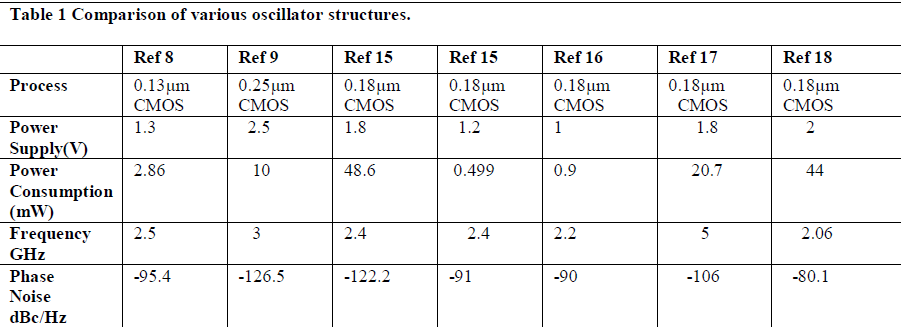
| In table 1we compare different oscillator structures i.e. oscillator based on band pass filter, active inductor, LC oscillator and ring oscillator. All oscillator structure has its own advantages and disadvantages. According to the need of application different oscillator are used. In this table all oscillator circuit is presented for different application. By comparing we get to know that LC oscillator has good phase noise as compared to ring but when comparing to other, other are good. Other oscillator structures improve tuning range, power consumption and area. |
 |
CONCLUSION |
| When we studied different structures here, we find that everyone has its own advantages and disadvantages. As result LC oscillator is preferable in RF communication due to its phase noise performance. While ring oscillator is used due to its wide tuning range, less silicon area but it is sensitive to power supply. But today new circuits replacing them and provide better results. In this paper a new RF oscillator design is proposed which can better meet the requirement of today’s applications. |
References |
|