Keywords
|
| Switching power converters, Conducted Emission, EMI filter. |
INTRODUCTION
|
| Conducted emissions from switching power converters has been a major problem in power electronics [5]. The sizes of the energy storage elements (transformers, inductors, and capacitors) in a Switching power converter decrease approximately linearly with the increase of the switching frequency [8]. Therefore, high-density power supplies generally demand high switching frequency and fast semiconductor devices. However, the increased switching frequency, together with the increased current and voltage slew rates, di/dt and dv/dt, have detrimental effects on the electromagnetic compatibility (EMC) performance of the power supplies. These effects are critical in the case of electronic packages in launch vehicle and should be carefully examined whether it meets required EMC standard. Electronic equipments handle transient energy in unpredictable ways. This is a major challenge. EMI practices usually take last-minute, trial-and-error experimental methods without careful planning and design. Furthermore, this lastminute patch-on solution sometimes cannot even meet the regulation requirement, which leads to malfunctioning or even failure of equipments and calls for redesign of the entire converter. |
| Conventionally, the total conducted EMI noise is caused by two mechanisms, the differential-mode (DM) and the common-mode (CM) noise. The source of differential mode (DM) interference is the current switched by a MOSFET or a diode. High rates of dv/dt and parasitic capacitors to the ground are the reasons for differential mode interferences. |
| EMI Filter is one of the most suitable methods for the mitigation of conducted EMI. This is illustrated in the block diagram below. |
| The design of an input filter starts with the measurements of the common mode (CM) and differential mode (DM) noise coming from the source of EMI – the Switching power converter in this case. This means that the power converter must be physically build before its input filter can be designed. A systematic design procedure is presented which considers common mode and differential mode sections separately. |
EMI FILTER DESIGN
|
| The design procedure is based on the knowledge of base-line common-mode (CM), and differential mode (DM) EMI. Conducted-emission tests have to be carried out first according to MILSTD 461C. The measuring current probe is used to separate the total conducted EMI into CM, and DM components, without the need for a special noise separator. |
INITIAL EMI MEASUREMENTS ON ACTUAL SYSTEM
|
| The line impedance stabilization network (LISN) purpose is to provide stabilized impedance to conducted emissions, without interfering with the normal power flow required by the equipment under test (EUT). At the power line frequency the LISN provides a low impedance path from the power source to the load impedance and a high impedance path from the load to ground. Major functions of LISN are |
| (1) Passing only the dc or ac power to the test sample, |
| (2) Preventing the test sample's electromagnetic noise from getting back in to the power bus, |
| (3) Blocking the power mains R-F from coupling into the test sample |
| During the conducted emission test, a LISN is placed between the product and the actual power line in order to present known impedance to the product's power line terminals over the frequency range of 150 KHz to 30MHz. One LISN is inserted in the hot side of the power line, and one is inserted in the neutral side of the power line. The circuit of a 50μH LISN used for most conducted emission testing is shown in Fig.3. |
| The 1μF capacitor C2 on the power line side of the LISN shorts out the variable impedance of the actual power line so that it does not influence the test results. The 50μH inductor L1 provides rising impedance with frequency. Capacitor C1 is used to couple the conducted emission measuring instrument to the power line. The 1000Ω resistor R1 discharges the LISN capacitors when the LISN is removed from the power line. Usually the measurements are carried out using two LISN circuits as shown in Fig-2. Noise levels are measured separately for line and neutral. If any of them fails to comply with the standard, the equipment is not EMC compatible. |
| Fig.4 shows a typical EMI filter configuration. Following are the general steps to design a baseline EMI filter |
| 1. The first step that must be considered in EMI filter design is accurate measurement of the emissions from line and neutral of the device under test by means of the measurement system. Then common mode and differential mode noise is calculated as |
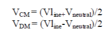 |
| 2. The second step is to determine the required CM-noise attenuation (Vreq,CM)dB and DM noise attenuation (Vreq,DM)dB using the following two equations: |
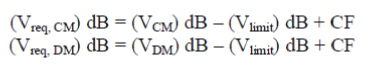 |
| Where (VCM) dB and (VDM) dB are the base line noise voltage from first step. (Vlimit) dB is the required conducted EMI limit specified by MIL STD 461C. CF (dB) denotes the correction factor of the designed method for avoiding design error. Usually +6dB is added because both the measured CM noise and DM noise using the present system are 3dB above the actual values, and because the measured CM and DM noise voltage may be in phase, which will cause a total error of 6dB in estimating the required attenuation. |
| 3.The third step is to determine the minimum corner frequency of second order L-C filter for CM and DM according to the attenuation requirement for all frequency spectrums. Fig.5 and Fig.6 show the EMI equivalent circuits for the CM noise and DM noise respectively, which take into account the effect of the 50Ω input impedance of the spectrum analyzer. |
| The ratio of the output power Po from a noise source without an L-C filter to the output power P'o from the same noise source with an L-C filter is defined as the attenuation (A) of this L-C filter. Since the output power is proportional to the square of the output voltage for the same load impedance, the attenuation (A) of an L-C filter in decibels (dBs) can be expressed as follows: |
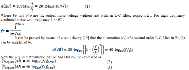 |
| Thus, the two corner frequency fR,CM and fR,DM in equations (2) and (3) correspond to the minimum intersection of the 40dB/decade slope along the frequency axis. |
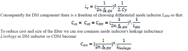
| 4. The final step in designing is to determine the inductor and capacitor component values (LCM, CCM) and (LDM, CDM) of the conducted EMI filter from the corner frequencies (fR,CM) and (fR,DM) found on the previous step. |
 |
| Fig.7, shows the steps for the proposed filter design procedure in summary |
| Filter component values are designed using graphical method described above. The EMI filter designed by this method may not be compact in size. [5] |
FILTER SIZE OPTIMIZATION
|
| To optimize the EMI filter size there are several considerations. Also common erroneous practices have to be avoided. Important aspects are |
GROUNDING
|
| CM noise propagates from the power circuit to ground. The impedance of this grounding connection has a great impact on the filter performance. Some key parameters affecting this impedance are whether wire or copper foil is used, and the actual length of the connection. The use of copper foils as ground interconnects helps reduce the CM noise in the system because they have smaller impedance. The copper foils have a lower inductance than the same length of wire. |
CM CHOKE SIZE OPTIMIZATION
|
| In order to achieve a high-density EMI filter, the size of the DM capacitors and CM choke needs to be minimized. There are inductor design methods that focus on the total space utilization. When designing inductance, the use of multilayer windings permits the use of much smaller cores, especially when thinner wire is used. At the same time, the use of multilayer windings changes the parasitics of the inductors, and hence, their behavior at HFs. Specifically, the effective parallel capacitance (EPC), which is the parasitic capacitance of the inductor winding, increases significantly. Nevertheless, a method such as that proposed in [15] could help to cancel out the EPC, achieving better performance at HFs. |
| Increasing the current density and using multilayer windings are effective ways to reduce the size of the CM choke and the entire filter volume. The total filter footprint is reduced nearly threefold. However, these methods have some drawbacks, such as a higher EPC and a higher operating temperature. The increase in temperature may be problematic for the application, and will affect the flux density saturation (Bsat ), which is a function of the temperature. Specifically, the Bsat of the ferrite core can become much lower at higher temperatures and lead to saturation due to the DM current; consequently, the impedance of the CM choke will be dramatically reduced and fail to meet the standard. A good way to avoid this unwanted performance is by using different magnetic materials, such as nanocrystalline cores, where the magnetic flux saturation is much higher [4] and the permeability does not change with respect to temperature. |
MAGNETIC CORE MATERIAL
|
| Nanocrystalline cores seem to be the most suitable material for CM chokes due to their high permeability, which is approximately three times higher than ferrite. So, the number of turns required to obtain the same inductance will be lower than using ferrite, which creates a much smaller leakage. The DM noise is greatly affected by this reduced leakage, the behavior of the nanocrystalline core at the midrange frequencies (between 10 and 250 kHz) where its permeability drops much faster than ferrite. The major advantage of using nanocrystalline core is its size reduction and behavior at HF. |
INTEGRATED CM AND DM INDUCTOR
|
| Integrated inductor configuration can be performed by placing a low-permeability core within the choke structure. Example, a Kool Mu core. It has the capability to increase the total leakage of the choke or DM inductance. The high permeability core mainly contributes to CM inductance, while the low-permeability core creates DM inductance. The integrated choke has better performance than the regular choke, with more attenuation. The same technique can also used successfully with a nanocrystalline core. The integrated inductor structure usually has a larger DM inductance than the multilayer winding structure, so the filter with this structure is more suitable for a power electronics system with high DM noise. When the DM noise is low enough such that a multilayer winding structure can provide enough DM inductance for DM noise attenuation, the multilayer winding structure would be a better choice. To minimize the total size of EMI filter, it is necessary to choose the correct filter components and use them close to their electrical, thermal, and mechanical limits. However, knowing the filter application and environment is also very important during the design stage.[20]. |
CONCLUSION
|
| A detailed study on conducted emissions from switching power converters is done. A systematic and practical EMI Filter design methodology is studied. This greatly reduces cut and trial effort in designing an EMI filter. Also various aspects to improve the performance of baseline filter are discussed. |
Figures at a glance
|
 |
 |
 |
 |
| Figure 1 |
Figure 2 |
Figure 3 |
Figure 4 |
 |
 |
 |
| Figure 5 |
Figure 6 |
Figure 7 |
|
| |
References
|
- Abdul Majid, JawadSaleem,KentBertilsson , “EMI Filter Design for High Frequency Power Converters”,2012
- Dong Jiang, Rixin Lai, Fei (Fred) Wang,FangLuo, Shuo Wang and DushanBoroyevich,, “Study of Conducted EMI Reduction for Three-Phase Active Front-End Rectifier”, IEEE TRANSACTIONS ON POWER ELECTRONICS, VOL. 26, NO. 12, DECEMBER 2011
- EberhardWaffenschmidt, Bernd Ackermann, and J. A. Ferreira , “Design Method and Material Technologies for Passives in Printed Circuit Board Embedded Circuits”,IEEE TRANSACTIONS ON POWER ELECTRONICS, VOL. 20, NO. 3, MAY 2005
- FINEMET CM Choke Cores, Technical Bulletin Metglas, Conway, SC,2004, p. 1.
- I.C adirci, B. Saka and Y. Eristiren, “Practical EMI-filter-design procedure for high-power high frequency SMPS according to MIL-STD 461”,2005
- Jean-Luc Kotny,XavierMargueron, Nadir Idir, “High Frequency Modeling Method of EMI filters”
- Klaus Raggl,ThomasNussbaumer,and Johann W. Kolar, “Guideline for a Simplified Differential-Mode EMI Filter Design”,VOL. 57, NO. 3, MARCH 2010
- Konstantin Kostov1 JormaKyyrä1 TeuvoSuntio2, “Analysis and Design of EMI Filters for DC-DC Converters Using Chain Parameters” 2003
- L. Kotny, X. Margueron ,N. Idir, “Coupling Inductor Models for EMI Filters”XuejunPel, JianXiong, Yong Kang and Jian Chen, “Conducted EM1 Emission in PWM inverter” 2002
- Marwan Ali, Eric Labour´e, Franc¸ois Costa and Bertrand Revol, “Design of a Hybrid Integrated EMC Filter for a DC–DC Power Converter”, IEEE TRANSACTIONS ON POWER ELECTRONICS, VOL. 27, NO. 11, NOVEMBER 2012
- P. Kong, S. Wang, C. Wang, and F. C. Lee, “Common-mode EMI study and reduction technique for the interleaved multichannel PFC converter,”IEEE Trans. Power Electron., vol. 23, no. 5, pp. 2576–2584, Sep. 2008.
- Q. Liu, S. Wang, F. Wang, C. Baisden, and D. Boroyevich, “EMI suppression in voltage source converters by utilizing DC-link decoupling capacitors,” IEEE Trans. Power Electron., vol. 22, no. 4, pp. 1417–1428,Jul. 2007
- Rengang Chen, J.D. van Wyk, Shuo Wang and W.G. Odendaal,“Technologies and Characteristics of Integrated EMI Filters for Switch Mode Power Supplies”, 2004
- Richard Lee Ozenbaugh and Timothy.M.Pullen, “EMI Filter Design”,CRC Press,2012,1.1-20.6
- S. Wang, F. Lee, and J. Wyk, “Inductor winding capacitance cancellation using mutual capacitance concept for noise reduction application,” IEEE Trans. Electromagn. Compat., vol. 48, no. 2, pp. 311–318, May 2006
- Sheng Ye, Wilson Eberle and Yan-Fei Liu, “A Novel EMI Filter Design Method for Switching Power Supplies”,2004.
- Sheng Liu, Yuting Zhang, Dayong Yu, “Research and Design of EMI Digital Filters Using Scattering Parameters”,2009
- Timothy C. Neugebauer and David J. Perreault, “Parasitic Capacitance Cancellation in Filter Inductors” 351h Annual IEEE Power Electronics Specialists Conference Aachen, Germany, 2004
- V.PrasadKodali, “Engineering Electromagnetic compatibility”, IEEE Press,1996,6-22,151-167,247-272.
- YoannMaillet, Rixin Lai, Shuo Wang, Fei (Fred) Wang, Rolando Burgos, DushanBoroyevich, “High-Density EMI Filter Design for DC-Fed Motor Drives”, IEEE TRANSACTIONS ON POWER ELECTRONICS, VOL. 25, NO. 5, MAY 2010
|