Keywords
|
| Reversible Logic, Reversible gate, Flip-Flop, Reversible counter. |
INTRODUCTION
|
| Reduction of power dissipation remains one of the major goals in the VLSI circuit design for many years. R.Landauer demonstrated in early 1960s, that irreversible hardware computation results in energy dissipation due to the information loss, regardless of its realization technique [2]. It is proved that the loss of each one bit of information dissipates at least KTln2 joules of energy (heat), where K is the Boltzmann’s constant and T is the absolute temperature at which operation is performed [2]. Reversible logic circuits have theoretically zero internal power dissipation since they have no information loss. Bennett showed that in order to avoid KTln2 joules of energy dissipation in a circuit, it must be built using reversible logic gates [3]. The applications of reversible logic are quantum computation [12], optical computing [13], ultra low power CMOS design [14] and nanotechnology [15]. |
| This paper is organized as follows. Section II presents a literature survey. Section III presents the basic definitions pertaining to reversible logic. Section IV discusses the reversible logic gates. Section V applications and Section VI conclude the paper. |
LITERATURE SURVEY
|
| Gordon. E. Moore [1] in 1965 predicted that the numbers of components on the chip will double every 18 months. Initially he predicted only for 10 years but due to growth in the integrated-circuit technology his prediction is valid till today. His work is widely recognized as the Moore's law. The effect of Moore's law was studied carefully and researchers have come to the conclusion that as the number of components in the chip increases the power dissipation will also increase tremendously. It is also predicted that the amount of power dissipated will be equal to the heat dissipated by the rocket nozzle. Hence power minimization has become an important factor for today's VLSI engineers. |
| Landauer [2] determined that the amount of energy dissipated to erase each bit of information is at least kTln2 (where k is the Boltzmann constant and T is the room temperature) during any computation the intermediate bits used to compute the final result are erased. This erasure of bits is one of the main reason for the power dissipation. |
| C. H. Bennett [3] in 1973 discovered that the power dissipation in any device can be made zero or negligible if the computation is done using reversible model. He proved his theory with the help of the turing machine which is a symbolic model for computation introduced by Turing. Bennett also showed that the computations that are performed on irreversible or classical machine can be performed with same efficiency on the reversible machine. Based on the above concept the research on the reversibility was started in 1980's. |
| In the year 1994 Shor [4] did a remarkable research work in creating an algorithm using reversibility for factorizing large number with better efficiency when compared to the classical computing theory. After this the work on reversible computing was started by more people in different fields such as nanotechnology, quantum computers and CMOS VLSI. |
| Edward Fredkin and Tommaso Toffoli [5, 6] based on the concept of reversibility they introduced new reversible gates known as Fredkin and Toffoli reversible gates. These gates have zero power dissipation and are used as universal gates in the reversible circuits. These gates have three outputs and three inputs, hence they are known as 3*3 reversible gates. |
| Peres [7] introduced a new gate known as peres gate. Peres gate is also a 3*3 gate but it is not a universal gate like the Fredkin and Toffoli gate. Even though this gate is not universal gate it is widely used in many application because it has less quantum cost when compared to the universal gate. The quantum cost of the Peres gate is 4. |
| H Thalpliyal and N Ranganathan [8] invented a reversible gate known as TR gate. The main objective of introducing this reversible TR gate was to reduce the garbage output in a reversible circuit. |
| Using the combination of Fredkin and Feynman gate a new gate known as Sayem gate was developed by Sujata S. Chiwande Prashanth R. Yelekar [10] sayem gate is a 4*4 reversible gate and is used in designing sequential reversible circuits. |
| Even though some significant works ([16] - [17], [18]) have been already done in the field of reversible sequential logic design, research on reversible counters has not been done. This paper proposes a novel concept on reversible sequential circuit design which includes asynchronous and synchronous counters. |
| H Thalpliyal and N Ranganathan [9] were the first people to introduce the reversible logic to sequential circuits. They were successful in implementing sequential circuit such as D-latch, T latch, JK latch and SR latch using Fredkin and Feynman gate. After this work more research has been done on sequential circuits using reversible gates. |
| M.L. Chuang and C.Y. Wang [11] proposed that the numbers of gates, the number of garbage output were reduced in implementing the Latches and when the results will be compared [9] with 25% improvement was achieved. Based on the above research and work done, we are going to implement the reversible logic concept for sequential circuits such as D-flip-flop, T-flip-flop and the four bit counters [9]. |
| V. Rajmohan and Dr. V. Ranganathan [22] in this be implemented counters using reversible logic. The synchronous and asynchronous counter designs have the applications in building reversible ALU, reversible processor etc. This work forms an important move in building large and complex reversible sequential circuits for quantum computers. |
PAGE BASIC DEFINITIONS PERTAINING TO REVERSIBLE LOGIC
|
| A. Reversible Function: |
| The multiple output Boolean function F(x1, x2,...,xn) of n Boolean variable is called reversible if: |
| 1. The number of outputs is equal to the number of inputs. |
| 2. Any output pattern has a unique pre-image. |
| In other words, the reversible functions are those that perform permutations of the set of input vectors |
| B. Reversible Logic Gate: |
| A reversible gate is a logical cell that has the N number of inputs and N number of outputs with a one-to-one mapping between the input and output vector. For the logical cell to be reversible the following two conditions are not permitted. |
| 1. Direct fan-outs from the reversible gates. |
| 2. Feedback from a gate output directly to its input. |
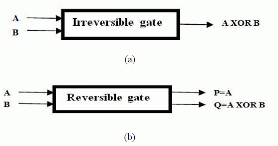
| The block diagram of irreversible XOR and reversible XOR gate is as shown in fig 1 |
| C. The number of Reversible gates (N): The number of reversible gates used in circuit. |
| D. The number of constant inputs (CI): This refers to the number of inputs that are to be maintained constant at either 0 or 1 in order to synthesize the given logical function. |
| E. The number of garbage outputs (GO): This refers to the number of unused outputs present in a reversible circuit. One cannot avoid the garbage outputs as these are very essential to achieve reversibility. |
| F. Quantum cost (QC): This refers to the cost of the circuit in terms of the cost of a primitive gate. It is calculated knowing the number of primitive reversible logic gates (1*1 or 2*2) required to realize the circuit. |
| G. Flexibility: This refers to the universality of a reversible logic gate in realizing more functions. |
| H. Gate Level: This refers to the number of levels in the circuit which are required to realize the given logic functions. |
| I. Hardware Complexity: This refers to the total number of logic operation in a circuit. Means the total number of AND, OR and EXOR operation in a circuit |
| J. Design Constraints for Reversible Logic Circuits: In the design of reversible logic circuits the following points must be considered to achieve an optimized circuit. |
| • Fan-out is not permitted. |
| • Minimum quantum cost. |
| • Garbage outputs must be minimum. |
| • Constant inputs must be minimum. |
| • Minimum number of logic depth or gate levels. |
| • Minimum delay. |
REVERSIBLE LOGIC GATES
|
| A reversible logic gate has equal number of input and output terminals and there is one to one mapping between them. Again we can say, gate is reversible if we can determine input vector from output vector and vice-versa. Reversible gate should practically loose very little amount of energy. Fan-out is not allowed in reversible circuits however fan-out can be achieved using additional gates. In this paper we have discussed basic reversible gate like Feynman gate, Fredkin gate, Toffoli gate, Peres gate and Sayem gate which we have used in implementing reversible sequential circuits. |
| 1. Feynman Gate: |
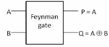
| Feynman gate is a 2*2 one through reversible gate as shown in figure 2. The input vector is I(A, B) and the output vector is O(P, Q). The outputs are defined by P=A, Q=A XOR B. Quantum cost of a Feynman gate is 1. Feynman Gate (FG) can be used as a copying gate. Since a fan-out is not allowed in reversible logic, this gate is useful for duplication of the required outputs [19]. |
| 2. Toffoli Gate: |
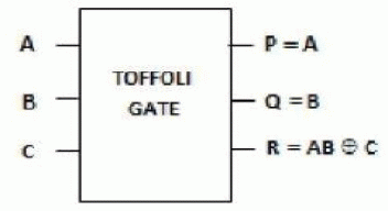
| Fig 3 shows a 3*3 Toffoli gate. The input vector is I (A, B, C) and the output vector is O(P,Q,R). The outputs are defined by P=A, Q=B, R=AB XOR C. Quantum cost of a Toffoli gate is 5[5]. |
| 3. Fredkin Gate: |
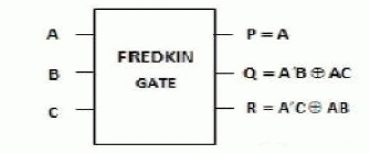
| Fig 4 shows a 3*3 Fredkin gate. The input vector is I (A, B, C) and the output vector is O (P, Q, R). The output is defined by P=A, Q=A′B XOR AC and R=A′C XOR AB. Quantum cost of a Fredkin gate is 5[6]. |
| 4. Peres Gate: |
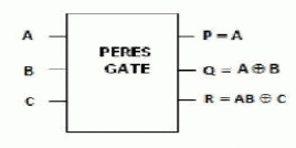
| Fig 5 shows a 3*3 Peres gate. The input vector is I (A, B, C) and the output vector is O (P, Q, R). The output is defined by P = A, Q = A XOR B and R=AB XOR C. Quantum cost of a Peres gate is 4[20]. |
| 5. Sayem Gate: |
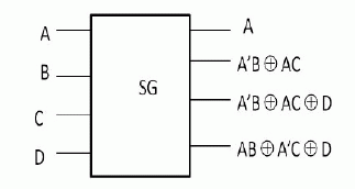
| Fig 6 shows 4x4 sayem gate. The input vector is I (A, B, C, D) and the output vector is O (P, Q, R, S). The output is defined by P=A, Q=A’B XOR AC, R=A’B XOR AC XOR D, S=AB XOR A’C XOR D [10]. |
| 6. LATCHES |
| Here we can use D-Latch or T-Latch depending upon choice that can be used in implementing reversible sequential circuit (counter) [21]. |
| I. D-LATCH: |
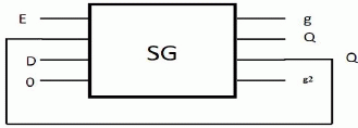
| The characteristic equation of D-Latch is Q+ =DE+E’Q. It can be realized with one SG. It can be mapped with SG by giving E, Q, D and 0 respectively in 1st, 2nd, 3rd and 4th input of SG. Fig 7(a) shows the design of D-Latch with only Q output and Fig 7(b) shows the design of reversible D-Latch with both the output Q and Q+ .One FG is needed to copy and produce the complement of Q from SG for the design of Fig 7(b) [24]. |
| II. T-Flip Flop |
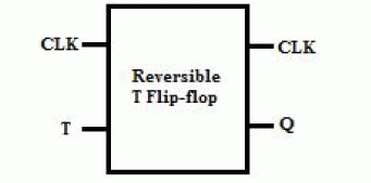
| As the name suggests, this flip-flop circuit used to toggle the output when input is high (1) and retains the output when input is low (0), thus it does two operation, it either holds the last state or toggles the output. Essentially, it has a logical symmetry with Controlled NOT kind operation. |
| The reversible realization of T Flip-flop has two SG gates and one Feynman Gate is shown in fig 8 [22]. |
| III. 4-BIT ASYNCHRONOUS UP/DOWN COUNTER: |
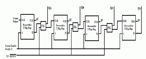
| The reversible design of the asynchronous Up/Down Counter is shown in Fig. 10[23]. The Up/Down operation of this reversible design is controlled by the control input UP/DOWN. When this control input is 1 the reversible design operates as an Up counter. When this control input is 0 the reversible design operates as a Down Counter [22]. |
APPLICATIONS
|
| Reversible computing may have applications in computer security and transaction processing, but the main long-term benefit will be felt very well in those areas which require high energy efficiency, speed and performance .it include the area like |
| • Low power CMOS. |
| • Quantum computer. |
| • Nanotechnology. |
| • Optical computing. |
| • DNA computing. |
| • Computer graphics. |
| • Communication. |
| • Design of low power arithmetic and data path for digital signal processing (DSP). |
| • Field Programmable Gate Arrays (FPGAs) in CMOS technology. |
CONLUSION AND FUTURE SCOPE
|
| The reversible circuits form the basic building block of quantum computers. This paper presents the primitive reversible gates which are gathered from literature and this paper helps researchers/designers in designing higher complex computing circuits using reversible gates. The paper can further be extended towards the digital design development using reversible logic circuits which are helpful in quantum computing, low power CMOS, nanotechnology, cryptography, optical computing, DNA computing, digital signal processing (DSP), quantum dot cellular automata, communication, computer graphics. |
| This work forms an important move in building large and complex reversible sequential circuits for quantum computers. The future work could be to develop efficient reversible counters and reversible controller circuits. |
Tables at a glance
|
|
|
| |
Figures at a glance
|
 |
 |
 |
 |
| Figure 1 |
Figure 2 |
Figure 3 |
Figure 4 |
 |
 |
 |
 |
| Figure 5 |
Figure 6 |
Figure 7 |
Figure 8 |
 |
 |
 |
| Figure 9 |
Figure 10 |
Figure 11 |
|
| |
References
|
- Gordon. E. Moore, Cramming more components onto integrated circuits Electronics, Volume 38, Number 8, April 19, 1965.
- Landauer .R, “Irreversibility and heat generation in the computing process”, IBM J. Research and Development, pp. 183-191, 1961.
- Bennett C.H., “Logical reversibility of Computation”, IBM J.Research and Development, pp. 525-532, 1973.
- P. Shor, Algorithms for quantum computation: discrete log and factoring, Proc. 35th Annual Symp. On Found. Of Computer Science (1994), IEEE Computer Society, Los Alamitos, 124-34.
- T. Toffoli., Reversible Computing, Tech memo MIT/LCS/TM-151, MIT Lab for Computer Science (1980).
- E. Fredkin and T. Toffoli, Conservative logic, Int. J. Theor.Phys., vol. 21, no. 3/4, pp.219 -253 1982.
- A. Peres, Reversible Logic and Quantum Computers, Physical Review A, vol. 32, pp. 3266-3276, 1985.
- H Thapliyal and N Ranganathan, Design of Efficient Reversible Binary Subtractors Based on a New Reversible Gate, IEEE Proceedings of the Computer Society Annual Symposium on VLSI, pp. 229-234 (2009).
- H Thapliyal and N Ranganathan, Design of Reversible Latches Optimized for Quantum Cost, Delay and Garbage Outputs, Proceedings of Twenty Third International Conferences on VLSI Design, pp. 235-240(2010).
- Sujata S. Chiwande and Prashanth R. Yelekar, Design of sequential circuit using reversible logic, IEEE-International Conference Advances in Engineering, Science and Management (ICAESM -2012) March30, 31, 2012.
- M. L. Chuang and C.Y. Wang, Synthesis of reversible sequential elements, ACM journal of Engineering Technologies in Computing Systems (JETC), vol. 3, no. 4, 2008.
- M. Nielson and I. Chuang, “Quantum Computation and Quantum Information”, Cambridge Univ. Press, 2000.
- E. Knill, R. Laflamme and G.J. Milbun,”A scheme for efficient quantum computation with linear optics”, Nature, vol. 409, no. 6816, pp. 46-52, 2001.
- G. Schrom, “Ultra-low-power CMOS Technology”, PhD thesis, technschenUniversitat Wien, June, 1998.
- R.C. Merkle, “Two types of mechanical reversible logic”, Nanotechnology, vol.4, pp. 114-131, 1993.
- P. Picton, “Multi-valued sequential logic design using Fredkin gates,” Multiple-Valued Logic Journal, vol. 1, pp. 241-251, 1996.
- Abu Sadat Md. Sayem and Masashi Ueda, “Optimization of Reversible Sequential Circuits,” Journal of Computing, vol.2, issue 6, pp. 208-214, 2010.
- SKS Hari, S Shroff, Sk Noor Mahammad and V. Kamakoti,”Efficient Building Blocks for Reversible Sequential Circuit design,” Proceedings of the International Midwest Symposium on Circuits and Systems, 2006.
- Md. BelayetAli , Md. MosharofHossin and Md. EneyatUllah, Design of Reversible Sequential Circuit Using Reversible Logic Synthesis International Journal of VLSI design & Communication Systems (VLSICS) Vol.2, No.4, December 2011.
- RakshithSaligram, Rakshith T.R, âÃâ¬Ãâ¢Novel Code Converter Employing Reversible logic,Volume 52– No.18, August 2012.
- Thapliyal H, Ranganathan N.," Design of Reversible Latches Optimized for Quantum Cost, Delay and Garbage Outputs" Centre for VLSI and Embedded System Technologies International Institute of Information Technology, Hyderabad, 500019, India.
- V.Rajmohan, V.Ranganathan,”Design of counter using reversible logic” 978-1-4244-8679-3/11/$26.00 ©2011 IEEE.
- M. Morris Mano, Michael D. Ciletti,” Digital Design,” fourth edition, Pearson Education, pp. 268-288.
- HimanshuThapliyal and N Ranganathan, “Design of Reversible Latches Optimized for Quantum Cost, Delay and Garbage outputs,” Proceedings of International Conference on VLSI Design, 2010.
|