Keywords
|
| Hybrid H-bridge, multicarrier phase-shifted pulse-width modulation, multilevel inverter, transistorclamped converter. |
INTRODUCTION
|
| Multilevel converters are mainly used to synthesis a required single or three-phase voltage waveform. The required multi-staircase output voltage is obtained by combining several balanced dc voltage sources. The most commonly used independent sources are Solar cells, fuel cells, batteries and ultra-capacitors [1]. One important application of multilevel converters is mainly concentrated on medium and high-power conversion systems. Now a day, there exist three commercial topologies of multilevel voltage-source inverters: neutral point clamped (NPC) or diode clamped inverter, cascaded H-bridge (CHB), and flying capacitors (FCs) [2]. Among these three topologies, cascaded multilevel inverter reaches the higher output voltage and power levels and the higher reliability due to its modular topology [3]. Diode-clamped multilevel converters are utilized in conventional high-power ac motor drive applications like conveyors, pumps, fans and mills. NPC also plays a vital role in oil, gas, metals, power, mining,and water, marine and chemical industries. In regenerative system also the NPC multilevel inverter is used in back to back configuration [4]. Flying capacitor multilevel converters have been used in high bandwidth high-switching frequency applications such as medium-voltage traction drives. Finally, hybrid cascaded H-bridge multilevel converters have been applied where high power and power quality are essential, for example, static synchronous compensators active filter, reactive power compensation applications, uninterruptible power supplies, photovoltaic power conversion and magnetic resonance imaging. One of the growing applications for multilevel motor drives is electric and hybrid power transient.For increasing voltage levels, the number of switches also will increase in number. Hence this leads to voltage stress and switching loss. For minimizing these losses we have to add filters, this process makes the circuit will become complex. By using the proposed topology, number of switches will reduce significantly and increase the efficiency of the system [5]. In high power applications, the harmonic content of the output waveforms has to be reduced as much as possible in order to avoid distortion in the grid and it will reach the maximum energy efficiency [6]. |
| The first multilevel inverter was introduced in three level converters. A multilevel converter is a power electronic system using several levels of dc voltages as inputs to synthesize a desired output voltage; the converter output voltage waveform approaches a nearly sinusoidal waveform while using a fundamental frequency-switching scheme. The primary advantage of multilevel inverter is their small output voltage, results in higher output quality, lower harmonic component, lower switching losses and better electromagnetic computability [7].The transistor clamped converter topology has received increased attention as it provides a simpler approach to increase output levels by taking different voltage levels from the series stacked capacitors [8 & 9]. In this paper, the proposed new configuration uses a thirteenlevel transistor-clamped H-bridge (TCHB) that can produce a thirteen-level output instead of five-level as with the conventional H-bridge[10-12]. A similar arrangement using a NPC in each power cell has been presented [13-17]. However, for the efficient output an excessive number of power switches and diodes are required. Cascaded hybrid H-bridge multilevel inverters increases the voltage levels, reduce losses and used for industrial application. The general configuration is shown in the figure 1.1 |
| In addition to the better output quality, with more output levels, the possibility of insulation failure is reduced across the motor terminals compared to the conventional CHB with similar configuration. It mainly focus on the constant speed drive applications such as fans, blowers, pumps and compressors, since these comprise 97% of currently installed medium voltage drives. It is found in various industries such as process industries, production plants as well as in oil and gas sectors.The proposed method mainly reduced the components used and concentrates on the better voltage utilization. It also reduces the switch counts, total harmonic distortion and reduces the losses. The figure 2.1 explains as follows, In order to converter the ac source into dc source rectifier is used in between the filter and ac source.The filter is mainly used to reduce the harmonics and other unwanted noise .The bypass series filter is mainly used for isolating purpose of the switches to be turned ON. Based on turning ON and turning off the switches the output voltage level is increased and the cascaded 13-level multilevel inverter is shown in the figure 2.2. |
| In general, the maximum levels in the phase and line voltages of the proposed inverter, based on NC (series-connected five levelsTCHB)cells, are given by the following equations. |
 (1) (1) |
 (2) (2) |
| Based on valid switching combinations - , the cell output voltage can be represented by |
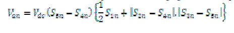 (3) (3) |
PWM MODULATION STRATEGY
|
| Pulse-Width Modulation (PWM) or pulse-duration modulation (PDM), is a modulation technique that controls the width (in time) of an electrical pulse, formally the pulse's duration, based on modulator signal information. Although this modulation technique can be used to encode information for transmission, its main use is to allow the control of the power supplied to electrical devices, especially to inertial loads such as motors. In addition, PWM is one of the two principal algorithms used in photovoltaic solar battery chargers, the other being MPPT. The modulation indexM of the proposed multilevelinverter isdefined by |
 (4) (4) |
| Where is the amplitude of the voltage reference and is the amplitude of the carrier signal. Multicarrier phase-shifted PWM (CPS-PWM) modulation is used to generate the PWM signals. |
| A.Phase Shift PWM (PSPWM) |
| The amplitude and frequency of all triangular carriers are the same as well as the phase shifts between adjacent carriers. In addition to the phase shift modulation, level shift modulations also exist in order to eliminate the harmonics of the output waveform. This scheme does not require any modification in the carrier or modulating signal. It has advantage or superiority over other previous works. But there is a phase shift between any two adjacent carrier waves. For m Voltage levels (m-1) carrier signals are required and they are phase shifted with an angle of θ=(360°/m-1). The gate signals are generated with proper comparison of carrier wave and modulating signal and it is shown in figure 3.1. |
| B. Level shifted PWM (LSCPWM) |
| For carriers signals, the time values of each carrier waves are set to [0 1/600 1/300] while the outputs values are set according to the disposition of carrier waves. After comparing, the output signals of comparator are transmitted to the IGBT. This technique is divided into 3 types,they are i)In Phase disposition (IPD) ii)Phase opposition disposition (POD)iii)Alternate phase opposition disposition (APOD) |
| i .In Phase disposition (IPD) |
| In this method all the carriers signals above and below zero reference line are in same phase. If all the carriers are selected with the same phase, then the method is known as Phase Disposition (PD) method. Carrier and reference wave arrangements are as shown in Fig.3.2. It is the most widely used strategy for Modular Multilevel converters and conventional multilevel inverters because it provides load voltage and current with lower harmonic distortion and switching losses. |
| ii.Phase opposition disposition (POD) |
| In this method all the carriers have the same frequency and the adjustable amplitude (unequal amplitude and difference with phase sequence). But all the carriers above the zero value reference are in phase among them but in opposition (180 degrees phase shifted) with those below. Carrier and reference wave arrangements are as shown in figure 3.3. |
| iii.Alternate phase opposition disposition (APOD) |
| In this method all the carriers have the same frequency and the adjustable amplitude (different or unequal amplitudes). There is 180 degree phase shift between all the carrier signals. |
| The carrier waves and the modulating signals are compared and the output of the comparator defines the output in the positive half cycle the comparator output will have the value high, if the amplitude of the modulating signal is greater than that of the carrier wave and zero otherwise and it is shown in figure3.4. Similarly for the negative half cycle, if the modulating signal is lower than the carrier wave the output of the comparator is high and zero otherwise. |
LINE-VOLTAGE THD
|
| Regarding the switching frequency of multilevel inverters, two categories are classified based on the switching strategies: strategies that work with high switching frequencies, including the classical carrier-based sinusoidal pulsewidth modulation (PWM) strategy, and those that work with low switching frequencies, generally equal to the fundamental component frequency, and generate a staircase waveform. Representatives of this category are the socalled “optimized harmonic stepped waveform”, “selective harmonic mitigation PWM” and “optimal minimization of the total harmonic distortion”. Although this category is not necessarily restricted to the fundamental frequency and higher switching frequencies can be employed in order to improve harmonic conditions, but in this section, fundamental frequency switching is considered. The extension can be made with higher switching frequencies categories. The most efficient method is OMTHD, by which the waveform THD is minimized by determining the switching angles while the desired fundamental component is generated. To achieve this, an optimization algorithm is employed, in which the objective is to minimize harmonics.THD and either the fundamental component is considered as a constraint or its error is added to the objective function .THD is defined as the ratio of all harmonic components rms value to the fundamental component value and is expressed as follows: |
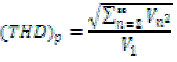 (5) (5) |
| The aim is to determine the optimum switching angles that generate an output voltage with the required fundamental component and the possible minimum THD. This is a problem to be solved by an optimization algorithm. |
| The above table shows the voltage and the total harmonic distortion for various multilevel inverters. |
| The figure 4.2 shows the total harmonics distortion (7.34%) for thirteenlevels. It is reduced from 29% to 7.34% for various levels. Along with the total harmonics distortion we are improving the output voltage with balanced dc source from 406V to 420V. |
ANALYSIS OF SIMULATION RESULTS
|
| The simulation result was analysed in both single and three phases by reducing the number of switches and the switch count with high efficiency and low power losses. In order to analysis the each level of multilevel inverter multicarrier phase shift pulse width modulation is used to reduce the harmonics of the output voltage waveform. In order to produce only the positive cycle waveform we have to activate the transistor clamped switches. For high power application mosfet is used as a switching device. The second order filter is used to reduce the output harmonics and it is shown in the figure 5.1. |
| In electronics, counters can be implemented quite easily using register-type circuits such as the flip-flop. The up/down counter is designed by JK flip-flop for producing toggle state. The up/down counters with NOT gate combination used to increment and decrement the levels both in positive and negative cycles. The multicarrier phase pulse width modulation is made with the comparison of fundamental and carrier signal. This makes the pulse width modulation in each level of the inverter. |
| Finally, with less number of switches the multilevel output is created for thirteen level with less harmonics and distortion. The harmonics distortion is reduced about 7.34% and it is shown in the figure 5.2. |
| The voltage is increased up to 420V. Normally the output is in the form sinusoidal waveform and it is shown in the figure 5.3.The distortion of a waveform relative to a pure sine wave can be measured either by using a THD analyser to analyse the output wave into its constituent harmonics and noting the amplitude of each relative to the fundamental; or the notch filter cancelling the fundamental and measuring the total aggregate harmonic distortion plus noise which will be the remaining signal. |
CONCLUSION
|
| In this paper, multilevel inverter configuration based on a thirteen-level TCHB inverter with multicarrier phase shifted PWM modulation technology, is analyzed and presented. A new method hybrid cascaded multilevel inverter was developed and tested with balanced DC source for better voltage utilization. The output voltages of the proposed inverter were analysed in various operating conditions. Detailed comparisons between the proposed inverter, NPC, 5LCHB and 9L-CHB in terms of power quality, power losses and total harmonic distortions also analysed. From the observations, the proposed inverter is found potential not only for medium-voltage drive application but also other applications like high voltage drives demanding higher output quality. |
Tables at a glance
|
 |
| Table 1 |
|
| |
Figures at a glance
|
 |
 |
 |
 |
| Figure 1 |
Figure 2 |
Figure 3 |
Figure 4 |
 |
 |
 |
 |
| Figure 5 |
Figure 6 |
Figure 7 |
Figure 8 |
 |
 |
 |
| Figure 9 |
Figure 10 |
Figure 11 |
|
| |
References
|
- Kavousi A, Vahidi B, Salehi R, Bakhshizadeh MA, Farokhnia N, et al. (2012) Application of the Bee Algorithm for Selective Harmonic Elimination Strategy in Multilevel Inverters. IEEE Trans 27: 1689-1696.
- Ahmadi D, KeZou, Li C, Huang Y, Wang J (2011) A Universal Selective Harmonic Elimination Method for High-Power Inverters IEEE Trans 26: 2743-2752.
- Filho F, Tolbert LM, Cao Y, Ozpineci B (2011) Real-Time Selective Harmonic Minimization for Multilevel Inverters Connected to Solar Panels Using Artificial Neural Network Angle Generation. IEEE Trans 47: 2117-2124.
- Sepahvand H, Liao J, Ferdowsi M (2011) Investigation on Capacitor Voltage Regulation in Cascaded H-Bridge Multilevel Converters With Fundamental Frequency Switching. IEEE Trans 58: 5102-5111.
- Wells JR, Patrick XG, Chapman L, Philip T, Brett K (2007) Modulation-Based Harmonic Elimination. IEEE Trans 22: 336-340.
- Napoles J, Watson AJ, Padilla JJ, Leon JI, Franquelo LG, et al (2012) Selective Harmonic Mitigation Technique for Cascaded H-Bridge Converters with Non-Equal DC Link Voltages. IEEE Trans 1-9.
- Rodriguez J, Lai J, Zheng F (2002) Multilevel Inverters: A survey of topologies, Control applications. IEEE trans 49: 724-738.
- Kouro S, Malinowski M, Gopakumar K, Pou J, Franquelo LG, et al (2010) Recent advances and industrial applications of multilevel converters. IEEE Trans Ind Electron 57: 2553–2580.
- Khomfoi S, Tolber t LM (2007) Fault diagnosis and reconfiguration for multilevel inverter drive using AI-based techniques.IEEETrans IndElectron 54: 2954–2968.
- Lezana P, Ortiz G (2009) Extended operation of cascade multicell converters under fault condition.IEEE Trans Ind Electron56: 2697–2703.
- Muruganandam M, Kumar NS, Sadasivam V (2007) A Low-cost Four-quadrant Chopper-fed Embedded DC Drive Using Fuzzy Controller. Inter National Journal of Electric Power Components and Systems, Taylor and Francis. 35: 907-920.
- Muruganandam. M, Thangaraju I and Madheswaran, M (2014) Simulation and Implementation of an Embedded Hybrid Fuzzy Trained Artificial Neural Network Controller for Different DC Motor. International Journal of Engineering and Technology6: 315-332.
- Muruganandam M, Madheswaran M (2009) Performance Analysis of Fuzzy Logic Controller Based DC-DC Converter fed DC Series Motor. IEEE international conference, Chinese Control and Decision Conference (CCDC 2009) 1635-1640.
- Raghav RK, Ramya R, Krishnaveni NV, Saravanan S (2014) Fault Tolerant FPGA Track Circuit for Railways Using Fuzzy Logic. International Journal of Scientific Progress and Research 5: 28-35
- Muruganandam M, Madheswaran M (2012) Simulation and Implementation of Generalized Hybrid Intelligent Controllers for Chopper fed DC Series Motor. International Journal of Wulfenia 19: 313-335.
- Nagarajan C, Muruganandam M, Ramasubramanian D (2012) Analysis and Design of CLL Resonant Converter for Solar Panel-battery Systems. International Journal of Intelligent Systems and Applications 1: 52-58.
- Saranraj S, Sasipriya A, Ramkumar S, Muruganandam M (2014) Voltage Controlled PFC SEPIC Converter Based PMBLDCM Drive for Air-Conditioners UsingFuzzy Controller. JAIR 3.
|