Keywords
|
| Boost converter, Zero voltage switching, Coupled inductor, Specific voltage gain, Soft switching technique, Inverter, Speed control of Induction motor |
INTRODUCTION
|
| DC–DC converters with high voltage gain are required in many industrial applications such as the front-end stage for the renewable and green energy sources including the solar arrays and the fuel cells, the power systems based on battery sources and super capacitors [1]–[6]. IN dc–dc converters with high voltage gain, there are several requirements such as high voltage gain [2], [3], [5], [6], low reverse-recovery loss [7], [8], soft-switching characteristic [16], low-voltage stress across the switches, electrical isolation, continuous input current, and high efficiency. In order to meet these requirements, various topologies are introduced. In order to extend the voltage gain, the boost converters with coupled inductors are proposed in [9] and [10]. The voltage gain is extended but continuous input current characteristic is lost and the efficiency is degraded due to hard switching of power switches. In [11], a step-up converter based on a charge pump and coupled inductor is suggested. Its voltage gain is around 10 but its efficiency is not high enough due to the switching loss. In [12], a high-step-up converter with coupled inductors is suggested to provide high voltage gain and a continuous input current. How- ever, its operating frequency is limited due to the hard switching of the switches. The converters suggested in [13]–[15] have a similar draw back. Their switching frequencies are limited due to the hard-switching operation. In order to increase the efficiency and power density, soft switching technique is required in dc–dc converters. In , various soft-switching techniques are suggested. Generally, there is a trade off between soft-switching characteristic and high voltage gain. It is because an inductor that is related with softswitching limits the voltage gain. In order to solve these problems, a zero-voltage-switching (ZVS) dc–dc converter with high voltage gain is proposed. As shown in Fig. 1, it consists of a ZVS boost converter stage to make the input current continuous and provide ZVS functions and a ZVS half-bridge converter stage to provide high voltage gain. Since single power processing stage can be a more efficient and cost-effective solution, both stages are merged and share power switches to increase the system efficiency and simplify the structure. Since both stages have the ZVS function, ZVS operation of the power switches can be obtained with wider load variation. Moreover, due to the ZVS function of the boost converter stage, the design of the half-bridge converter stage can be focused on high voltage gain. Therefore, high voltage gain is easily obtained. ZVS operation of the power switches reduces the switching loss during the switching transition and improves the overall efficiency. The theoretical analysis is verified by a 100W experimental prototype with 24–393 V conversion. |
ANALYSIS OF THE PROPOSED CONVERTER
|
| The equivalent circuit of the proposed converter is shown in Fig. 2. The ZVS boost converter stage consists of a coupled inductor Lc , the lower switch Q1, the upper switch Q2, the auxiliary diode Da, and the dc-link capacitor Cdc. The diodes DQ1 and DQ2 represent the intrinsic body diodes of Q1 and Q2. The capacitors CQ1 and CQ2 are the parasitic output capacitances of Q1 and Q2. The coupled inductor Lc is modelled as the magnetizing inductance Lm1, the leakage inductance Lk1, and the ideal transformer that has a turn ratio of 1:n1 (n1 = Ns1/Np1). The ZVS halfbridge converter stage consists of a transformer T, the switches Q1 and Q2, the output diodes Do1 and Do2, the dcblocking capacitors CB1 and CB2, and the output capacitor Co. The transformer T is modelled as the magnetizing inductance Lm2, the leakage inductance Lk2, and the ideal transformer that has a turn ratio of 1:n2 (n2 = Ns2/Np2). The practical waveforms of the proposed converter are shown in Fig. 3. The switches Q1 and Q2 are operated asymmetrically and the duty ratio D is based on the switch Q1. The operation of the proposed converter in one switching period Ts can be divided into seven as shown in Fig. 4. Just before Mode 1, the upper switch Q2, the auxiliary diode Da, and the output diode Do1 are conducting. The magnetizing current im1 of Lc arrives at its minimum value Im12 and the auxiliary diode current iDa arrives at its maximum value IDa. The current iL has its maximum value IL1. |
MODES OF OPERATION
|
| The DC-DC converter is operated in several modes for the production of high and specific voltage gain. The modes of operation can be explained by a single module as shown in figure 2. |
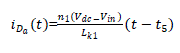
| Mode1[t0,t1]: At t0, the upper switch Q2 is turned OFF. Then, the capacitor CQ2 starts to be charged and the voltage vQ2 across Q2 increases toward Vdc. Simultaneously, the capacitor CQ1 is discharged and the voltage vQ1 across Q1 decreases toward zero. With an assumption that the output capacitances CQ1 and CQ2 of the switches are very small and all the inductor currents are not changed, the transition time interval Tt1 can be considered as follows: |
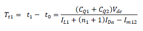 |
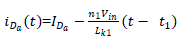
| Mode2[t1,t2]: At t1, the voltage vQ1 across the lower switch Q1 becomes zero and the body diode DQ1 is turned ON. Then, the gate signal for Q1 is applied. Since the current has already flown through the body diode DQ1 and the voltage vQ1 is maintained as zero before the switch Q1 is turned ON, the zero-voltage turn-ON of Q1 is achieved. Since the voltage vp1 across the magnetizing inductance Lm1 is Vin, the magnetizing current im1 increases linearly from its minimum value Im 2 as follows: |
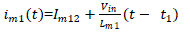 |
| Since the voltage vLk1 across the leakage inductance Lk1 is –(n1Vin+Vdc), the auxiliary diode current iDa linearly decreases from its maximum value IDa as follows: |
 |
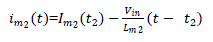
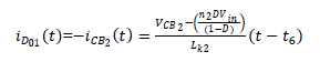
| Mode 3 [t2,t3]: At t2, the current iCB2 changes its direction. The output diode current iDo1 decreases to zero and the diode Do1 is turned OFF. Then the output diode Do2 is turned ON and its current increases linearly. Since the current changing rate of Do1 is controlled by the leakage inductance Lk2 of the transformer T, its reverse-recovery problem is alleviated. Since vp2 is the same as in Mode 2 and vLk2 is n2Vin+VCB2–Vo,the current im2 and the diode current iDo2 are given by |
 |
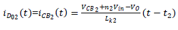 |
| The currents ip2, iL, and iQ1 can be obtained from the same relations in Mode 2. In this mode, the voltages vp1 and vLk are equal to those in Mode 2. Therefore, the magnetizing current im1, the auxiliary current iDa, and the input current iin change with the same slopes as in Mode 2. |
| Mode4[t3,t4]: At t3, the auxiliary diode current iDa decreases to zero and the diode Da is turned OFF. Since the changing rate of the diode current iDa is controlled by the leakage inductance Lk1 of the coupled inductor Lc, its reverse-recovery problem is alleviated. Since the voltage vp1 across the magnetizing inductance Lm1 is the input voltage Vin, the mag-netizing current im1 increases linearly with the same slope as in Modes 2 and 3 as follows: |
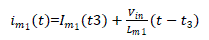 |
| Since the auxiliary diode current iDa is zero, the input current iin is equal to the magnetizing current im1. At the end of this mode, the magnetizing current im1 arrives at its maximum value Im11. Since the voltages vp2 and vLk2 are not changed in this mode, the slopes of the current im2, iCB2, and iL are not changed. |
| Mode5[t4,t5]: At t4, the lower switch Q1 is turned OFF. Then, the capacitor CQ1 starts to be charged and the voltage vQ1 across Q1 increases toward Vdc. Simultaneously, the capacitor CQ2 is discharged and the voltage vQ2 across Q2 decreases toward zero. With the same assumption as in Mode 1, the transition time interval Tt2 can be determined as follows: |
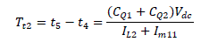 |
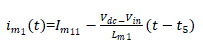
| Mode 6 [t5,t6]: At t5, the voltage vQ2 across the upper switch Q2 becomes zero and the body diode DQ2 is turned ON. Then, the gate signal is applied to the switch Q2. Since the current has already flown through the body diode DQ2 and the voltage vQ2 is maintained as zero before the turn-ON of the switch Q2, the zero-voltage turn-ON of Q2 is achieved. Since the voltage vp1 across the magnetizing inductance Lm1 is –(Vdc–Vin), the magnetizing current im1 decreases linearly from its maximum value Im11 as follows: |
 |
| Since the voltage vLk1 across the leakage inductance Lk is n1(Vdc–Vin), the auxiliary diode current iDa linearly increases from zero as follows: |
 |
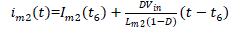
| Mode 7 [t6,t7]: At t6, the current iCB2 changes its direction. The output diode current iDo2 decreases to zero and the diode Do2 is turned OFF. Then the output diode Do1 is turned ON and its current increases linearly. Similar to Do1, the current changing rate of Do2 is controlled by the leakage inductance Lk2 of the transformer T and its reverserecovery problem is alleviated. Since vp2 is the same as in Mode 6 and vLk2 is VCB2– n2DVin/(1–D), the current im2 and the diode current iDo2 are given by |
 |
 |
| The currents ip2 and iL can be obtained from the same relations in Mode 2. In this mode, the voltages vp1 and vLk1 are equal to those in Mode 6. Therefore, the magnetizing current im1, the auxiliary current iDa, and the input current iin change with the same slopes as in Mode 2. |
INVERTER OPERATION AND ANALYSIS
|
| The adoption of AC power has created a trend where most devices adapt AC power from an outlet into DC power for use by the device. However, AC power is not always available and the need for mobility and simplicity has given batteries an advantage in portable power. Thus, for portable AC power, inverters are needed. Inverters take a DC voltage from a battery or a solar panel as input, and convert it into an AC voltage output. |
| There are types of DC/AC inverters available which are classified by their output type. Pure sine wave inverters offer more accuracy and less unused harmonic energy delivered to a load, but they are more complex in design and more expensive. Pure sine wave inverters will power devices with more accuracy, less power loss, and less heat generation. |
| Pure sine wave inversion is accomplished by taking a DC voltage source and switching it across a load using an H-bridge. If this voltage needs to be boosted from the DC source, it can be accomplished either before the AC stage by using a DC-DC boost converter, or after the AC stage by using a boost transformer. The inverted signal itself is composed of a pulse-width-modulated (PWM) signal which encodes a sine wave shown in figure 4. The duty cycle of the output is changed such that the power transmitted is exactly that of a sine-wave. This output can be used as-is or, alternatively, can be filtered easily into a pure sine wave. This report documents the design of a true sine wave inverter, focusing on the inversion of a DC high-voltage source. It therefore assumes the creation of a DC-DC boost phase. |
3-LEVEL PWM
|
| In order to create a signal which is closer to a true sine wave, a 3 level PWM signal can be generated with high, low, and zero voltage levels. For the resulting 3-level PWM signal to correspond to a sine wave, the signal comparison stage must also be 3-level . A triangle wave is used as it is in the 2-level PWM comparison, but it half the amplitude and summed with a square wave to compare one half of the sine reference signal at a time. The resulting PWM signal is used to controls how long the bus voltage is allowed through to the load. The bridge controls the polarity of the voltage across the load, and is controlled by a simple square wave of the same frequency and in phase with the sine signal. Generally, this square wave can simply be created in a stage of the sine wave generation circuit. A virtual example of such a 3-level circuit we simulated is shown in figure . The resulting 3-level high-voltage PWM signal shown in figure 5 can be filtered into a very close approximation of the sine wave as shown in figure 6. It should be noted that the simulations we did for this technique utilized a very low switching frequency for the triangle wave, so the PWM switching frequency is also low. This was done so that the waveforms would be easy to view and understand. In reality, a switching frequency above 20 kHz would be used to keep inductance ringing outside the range of human hearing. |
OPERATION AND SPEED CONTROL OF 3-PHASE INDUCTION MOTOR
|
| The voltage and torque equations that describe the dynamic behaviour of an induction motor are time-varying. It is successfully used to solve such differential equations and it may involve some complexity. A change of variables can be used to reduce the complexity of these equations by eliminating all time-varying inductances, due to electric circuits in relative motion, from the voltage equations of the machine . By this approach, a poly phase winding can be reduced to a set of two phase windings (q-d) with their magnetic axes formed in quadrature. In other words, the stator and rotor variables (voltages, currents and flux linkages) of an induction machine are transferred to a reference frame, which may rotate at any angular velocity or remain stationary. Such a frame of reference is commonly known in the generalized machines analysis as arbitrary reference frame The dynamic analysis of the symmetrical induction machines in the arbitrary reference frame has been intensively used as a standard simulation approach from which any particular mode of operation may then be developed. Mat lab/Simulink has an advantage over other machine simulators in modelling the induction machine using dq axis transformation. It can be a powerful technique in implementing the machine equations as they are transferred to a particular reference frame. Thus, every single equation among the model equations can be easily implemented in one block so that all the machine variables can be made available for control and verification purposes. In this paper, Mat lab/Simulink is used to simulate the dynamic performance of an induction motor model whose stator and rotor variables are referred to an arbitrary reference frame. The provided machine model is simulated in a way that makes it easy for the reader to follow and understand the implementation process since it gives full details about Simulink structure of each of the model equations. |
| In this section, the three phase induction machine model is simulated by using the Mat lab/Simulink. The Model is implemented using the same set of equations provided. The figure 7 below depicts the matlab modelling of the Induction motor. |
SIMULATION RESULTS
|
| The following model is the main circuit for proposed model. |
| The output of the inverter consist of harmonics. Total harmonic distortion of this model is not considered here since the concern is about driving the 3-Phase load. |
INDUCTION LOAD
|
| A 3-Phase Induction motor is used as test load in this module. The figure 8 and figure 9 shows the proposed model and torque and speed characteristics of the Induction motor respectively. |
RATING OF INDUCTION MOTOR
|
| 1. 5 HP |
| 2. Synchronous speed=1500 |
| 3. Rotor speed =1466 rpm |
| 4. Torque =5 N-M |
| 5. Slip= 2.26 % |
EXPERIMENTAL RESULTS
|
| The theoretical analysis of the proposed dc–dc converter, the input voltage Vin and the output voltage Vo are 24 V and 393 V, respectively. The switching frequency of the mosfet fs is 108 kHz. The circuit parameters can be selected as per design requirement of the proposed model. The turn ratio n1 of the coupled inductor Lc is calculated . By choosing a proper d1, the turn ratio n1 can be determined. Here, d1 is chosen as 0.88 and n1 is selected as n = 0.5. are selected .The leakage inductance Lk1 of the coupled inductor Lc can be determined. In order to obtain ZVS regardless of the load condition, Lk1 needs to be designed to satisfy the ZVS condition at full load. Lk1 is selected as 16.75 μH. Then the magnetizing inductance Lm1 is designed as 800 μH with I∗ = 2.7 A. According to α, the leakage inductance Lk2 of the transformer T is selected as 170 μH. The magnetizing inductance Lm2 of the transformer T is selected as 474 μH. The dc-blocking capacitors CB1 and CB2 are 6.6 μF and 2.2 μF, respectively. Fig. 3 shows the experimental waveforms of the prototype . Since the input current iin does not change its direction, the proposed converter operates in CCM. The dc-link voltage Vdc is around 85 V. |
| Therefore, the voltage stresses of the power switches are confined to 85 V. It can be seen that the experimental waveforms agree with the theoretical analysis. The proposed ZVS dc–dc converter exhibits an efficiency of 94.5% at the full load condition. The efficiency was improved by 2.4% compared with the conventional non isolated boost converter with a coupled inductor for a high voltage gain [8]. In addition, the efficiency of the modified version of the proposed converter is plotted. In the modified version, the input stage of the proposed converter is changed with the conventional CCM boost converter and the half-bridge converter stage is redesigned. The efficiency of the proposed converter with the ZVS boost converter stage is higher than those of the others under from 20% to 100% load . However, the efficiency of the proposed converter at light load is lower due to the additional conduction loss of the auxiliary circuitry of the ZVS boost converter stage. The output of the ZVS boost converter is 393 DC. |
| The inverter operation converts 393 V DC to a 400 V AC output at final stage. The output of the inverter though contains distortion, THD was not reduced. The 400 V AC supply is fed to a 3-Phase Squirrel cage Induction motor for operation and speed control. A Constant torque of 5 N-m is fed as input to the motor along with the AC input. The speed obtained was 1466 with a slip of 2.26% . A trial was done with torque of 4 N-m the speed obtained is 1474 with slip of 1.73 % . |
CONCLUSION
|
| A ZVS dc–dc converter with high voltage gain was suggested. It can achieve ZVS turn-ON of two power switches while maintaining CCM. In addition, the reverse-recovery characteristics of the output diodes were significantly improved by controlling the current changing rate with the use of the leakage inductance of the transformer. The proposed converter presents a higher efficiency and a wider ZVS region compared to other softswitching converters due to the ZVS boost converter stage. . The output of the ZVS boost converter is fed to the inverter for AC output at final stage.. The AC supply is fed to a 3-Phase Squirrel cage Induction motor for operation and speed control to obtain a constant speed and torque. |
| |
Figures at a glance
|
 |
 |
 |
 |
 |
| Figure 1 |
Figure 2 |
Figure 3 |
Figure 4 |
Figure 5 |
 |
 |
 |
 |
| Figure 6 |
Figure 7 |
Figure 8 |
Figure 9 |
|
| |
References
|
- F. Blaabjerg, Z. Chen, and S. B. Kjaer, “Power electronics as efficient interface in dispersed power generation systems,” IEEE Trans. Power Electron., vol. 19, no. 5, pp. 1184–1194, Sep. 2004.
- R. J. Wai, W. H. Wang, and C. Y. Lin, “High-performance stand-alone photovoltaic generation system,” IEEE Trans. Ind. Electron., vol. 55, no. 1, pp. 240–250, Jan. 2008.
- R. J. Wai and W. H. Wang, “Grid-connected photovoltaic generation sys- tem,” IEEETrans.CircuitsSyst.I,Reg.Papers,vol.55,no.3,pp.953–964, Apr. 2008.
- R. J. Wai, C. Y. Lin, C. Y. Lin, R. Y. Duan, and Y. R. Chang, “High- efficiency power conversion system for kilowatt-level distributed generation unit with low input voltage,” IEEE Trans. Ind. Electron., vol. 55, no. 10, pp. 3702–3714, Oct. 2008.
- S. K. Mazumder, R. K. Burra, and K. Acharya, “A ripple-mitigating and energy-efficientfuelcellpowerconditioningsystem,” IEEETrans.Power Electron., vol. 22, no. 4, pp. 1437–1452, Jul. 2007.
- 6 K. Kobayashi, H. Matsuo, and Y. Sekine, “Novel solar-cell power sup- ply system using a multiple-input DC–DC converter,” IEEE Trans. Ind. Electron., vol. 53, no. 1, pp. 281–286, Feb. 2006.
- Q. Zhao, F. Tao, F. C. Lee, P. Xu, and J. Wei, “A simple and effective to alleviate the rectifier reverse recovery problem in continuous-currentmodeboostconverter,” IEEEPowerElectron.,vol.16,no.5,pp.649–658, Sep. 2001.
- Q. Zhao and F. C. Lee, “High-efficiency, high step-up dc–dc converters,” IEEE Power Electron., vol. 18, no. 1, pp. 65–73, Jan. 2003.
- Q. Zhao, F. Tao, Y. Hu, and F. C. Lee, “Active-clamp DC/DC converter using magnetic switches,” in Proc. IEEE Appl. Power Electron. Conf., 2001, pp. 946–952.1586 IEEE TRANSACTIONS ON POWER ELECTRONICS, VOL. 26, NO. 5, MAY 2011
- D. A. Grant, Y. Darroman, and J. Suter, “Synthesis of tapped-inductor switched-mode converters,” IEEE Trans. Power Electron., vol. 22, no. 5, pp. 1964–1969, Sep. 2007.
- K. I. Hwu and Y. T. Yau, “Voltage-boosting converter on charge pump and coupling inductor with passive voltage clamping,” IEEE Trans. Ind. Electron., vol. 57, no. 5, pp. 1719–1727, May 2010.
- S. V. Araujo, R. P. Torrico-Bascope, and G. V. Torrico-Bascope, “Highly efficient high step-up converter for fuel-cell power processing based on three-state commutation cell,” IEEE Trans. Ind. Electron., vol. 57, no. 6, pp. 1987–1997, Jun. 2010.
- C.-T. Pan and C.-M. Lai, “A high-efficiency high step-up converter with low switch voltage stress for fuel-cell system applications,” IEEE Trans. Ind. Electron., vol. 57, no. 6, pp. 1998–2006, Jun. 2010.
- S.-K. Changchien, T.–J. Liang, J.-F. Chen, and L.-S. Yang, “Novel high step-up DC-DC converter for fuel cell energy conversion system,” IEEE Trans. Ind. Electron., vol. 57, no. 6, pp. 2007–2017, Jun. 2010.
- H.Cheng,K.M.Smedley,andA.Abramovitz,“Awide-input-wide-output (WIWO) DC-DC converter,” IEEE Trans. Power Electron., vol. 25, no. 2, pp. 280–289, Feb. 2010.
|