An Application Specific Integrated Circuit (ASIC) for dual axis robotic motion control was designed and developed with Computer Aided Design (CAD) tools. The ASIC provides an all-digital dual-axis Pulse Width Modulated (PWM) amplifier interface. The ASIC layout was produced on a SUN workstation using all design tools. A standard cell library of basic digital functions and an automatic placement and autorouting program was used in the course of the design. The design was implemented in 2-micron Scalable CMOS (SCMOS) technology through the Metal Oxide Semiconductor implementation Service (MOSIS). The device was fabricated in both 40-pin ceramic DIP and 44-pin Plastic Leaded Chip Carrier (PLCC) packages. The dual-axis PWM controller chip was designed as part of a complete dual-arm, forcereflecting, master-slave telerobotic manipulator system and provides a 24 KHz PWM drive signal and control for a twoaxis, 500-watt amplifier module. The device interfaces to a microprocessor bus and requires only 100 MW of power at 12 MHz operation.
INTRODUCTION |
| The continued advancement of large scale integrated circuit processing technology and computer aided design tools have
provided the capability to design cost-effective custom integrated circuits with a high degree of success. Steady advances in
the level of integration in electronic circuits have improved many aspects of production equipment-improve reliability,
reduced costs, easier fabrication, increased performance, and lower power consumption. The use of VLSI circuits have
enabled manufacturers to provide such impressive devices as battery operated Compact Disc players barely larger than the
diameter of the disc itself And able to provide hours of music listening pleasure. The benefits of custom VLSI design are
variable and depend on the application and volume production requirements. With all the benefits that VLSI designs afford,
though many designers have hesitated to use Asics because of the initial high-price and risk associated with VLSI designs.
In addition, VLSI design centers generally require a firm commitment for the number of integrated circuits that will be
purchased. The initial investment, NRE costs and design time push designers to opt for discrete circuit designs using Small
Scale Integration (SSI) and Medium Scale Integration (MSI) integrated components resulting in increased circuit board area
and power dissipation. Many designers are using Programmable Array Logic (PAL) devices to replace the unavoidable
"glue-logic'' and to save board space. |
THE ADVANCED TELEROBOT MANIPULATOR |
| The dual-axis PWM controller chip was designed as part of a complete dual-arm, force-reflecting, master-slave telerobotic
manipulator system. The Advanced TeleRobot is a 7 degree-of-freedom manipulator with force reflecting feedback
capabilities. Each joint of the manipulator consists of a pitch/yaw mechanism requiring two drive systems to accomplish a
two degree-of-freedom motion. The PWM ASIC controller provides the PWM drive signal and control for a two-axis, 500-
watt amplifier module that drives the two motors of each manipulator joint. By co-locating the servo control and amplifier
electronics in the joint structure, the manipulator joints are made electrically and mechanically interchangeable. The result
is a telerobotic manipulator arm that is adaptable, modular, and easily maintained. Distributed axis telerobotic manipulator
control is the target of this research effort. Distributed motion control is made possible with the recent advances in
microcontroller technology and standard cell VLSI design tools. Distributed co-located control architecture was developed
and implemented for the Advanced TeleRobot System. A Dual-Axis Manipulator Element (DAME) was designed as a set
of three 10.16 cm (4-inch) diameter circuit boards for mounting within the manipulator arm module. The microprocessorbased
servo-control and amplifier electronics are packaged within the manipulator joint co-located with the drive motors
and motion sensors. Modularity and interchangeability of manipulator * Minimizes the number of conductors routed
through the Increased reliability of the mechanical interconnection, Improved command throughput via the utilization of
independent joint controllers for each axis, and Local servo control provides increased processing bandwidth. elements, arm
thereby reducing cable handling and increasing cable reliability, The reliability and the long term stability of the control
system is further enhanced by the implementation of a totally digital control system. This is achieved by using digital PWM servo control amplifiers and digital optical position encoders mounted directly on the motors. Velocity is calculated using a
discrete time derivative of the position data. Since no analog transducer interfacing is used in the design, long term stability
and reliability is improved. |
ASIC DESIGN REQUIREMENTS |
| The initial goal of the ASIC design itself was to replace many of the required interface components that are needed for
distributed servo-control electronics. An often used sensor is the quadrature phase incremental optical encoder. These
sensors provide low-inertia, low-friction, and high reliability position sensing. They are normally mounted directly to the
motor shafts. These type of encoders provide efficient and economical means for obtaining position and velocity. These
encoders can be obtained with resolutions of 64 to 2048 counts per revolution for low cost, general purpose applications.
Motor amplifiers are most often PWM type amplifiers that require an analog interface for the feedback and drive command.
The distributed control approach necessitates a Digital-to-Analog (D/A) converter for each motor within the joint. Noise
becomes a potential problem from the standpoint of design and layout because of the digital electronics. Again, there is
always limited space available to allow distribution of the servo electronics. Brush type motors are used and these also emit
a large amount of electrical noise. During the initial design efforts, a commercial PWM amplifier (the AMC-250D from
Advanced Motion Controls) was found that would fit within the dimensional constraints of the manipulator arm. The AMC-
250D was specially designed for TRI to accept a digital PWM drive signal command. The amplifier measures only
4.25x5.0x1.27 centimeters in size and provides up to 250 watts of power. |
PERFORMANCE OBJECTIVES |
| The performance objectives that were sought in the design of the ASIC interface controller were the PWM resolution and
the PWM base frequency. The desired PWM frequency was specified to be a minimum of 20 KHz. The desire to use PWM
amplifiers with 20 KHz base frequency provides efficient power dissipation and improved form factor for the system. The
power loss PL in a DC motor can be expressed in terms of the form factor (k) and the average current IAVG. The form
factor is expressed as: |
| K=IRMS/IAVG |
| And the power loss is expressed as: |
| PL = Rk2/AvG2 |
| Thus the armature losses in the motor depend on the average current, the form factor, and the armature resistance. The
resistance is fixed and the average current determines the torque output of the motor. Therefore, the additional heat losses in
the motor increase as the square of the form factor so that with a form factor of only 1.1, the armature losses are increased
by 21 percent degrading the torque capability of the motor. By using higher PWM frequencies, the RMS current becomes
more nearly equal to the average current and the form factor approaches unity. Another advantage of the PWM amplifier is
the reduced power dissipation in the amplifier itself. This is important since the amplifiers are packaged within the arm
module with the motors and control electronics. Additionally, the audio noise of the motor-amplifier system is eliminated
since 20 KHz is above the auditory response of humans. The minimum acceptable resolution of the PWM signal was
specified to be 10-bits. The drive command from the microprocessor is represented as -512 to +511 with 0 representing 50
percent duty cycle and no commanded torque to the motor. This resolution provides a signal to noise ratio greater than 60
dB. Since the manipulator is designed for force reflection, it is important to have good dynamic range to control the forcefeedback
effect of the manipulator. Since the PWM is implemented digitally, the theoretical input frequency of the ASIC
can be calculated as follows: |
| Input Frequency = 21° x 20 KHz ( 3 ) |
| Using equation (3) the ASIC must operate at a frequency of 20.48 MHz for a 10 bit resolution implementation. |
ASIC DESIGN PROCESS |
| The design and development process of this ASIC reveals the advances that are rapidly being made in the area of
microelectronics. The design of the ASIC represents a four step process from the standpoint of the hardware
implementation. |
Breadboard Testing |
| The ASIC design began with a conceptual design and a breadboard of the ASIC from available discrete components. The
initial component blocks of the ASIC were designed and simulated using the Douglas CAD/CAM package available from
Douglas Electronics. The circuit was then breadboarded on a 15 by 22 centimeter perfboard using readily available SSI and
MSI components. Only one of the optical encoder interfaces and PWM drive circuits was included in the breadboard
testing. Some of the microprocessor interface circuitry and decoding logic was also included. The breadboard design indicated that approximately 80 SSI and MSI components would be needed for the discrete version of the ASIC. Custom
The design was implemented on a SUN workstation using custom VLSI CAD design tools. The ASIC design and layout
was done using Berkeley's VLSIICAD software package. Two programs titled Magic and DRC (Incremental Design Rule
Checker) were used for the layout and routing. Extensive simulation was performed using SPICE and other simulation
programs for event-driven, switch-level, and worst case timing simulation. A program for automatic generation of
Programmable Logic Array (PLA) type blocks was also used to implement the control and decoding functions within
DARC. The first layout attempt produced a 64-pin ceramic DIP package that was about 60 percent functional. Timing
difficulties in the high speed switching circuitry limited the functionality of the majority of the circuit. Th e design was
implemented in 3-micron, double-metal CMOS. An automatic PIA generation and layout program was used to generate the
decoding and control logic. The final design resulted in a 64-pad die with external dimensions of 4600x6800 micron2 and
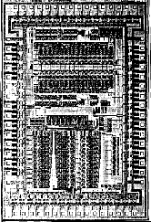
internal available silicon area of 3330x5520 micron2. MOSIS is show below in Figure 1. The chip was fabricated using a 3-micron p-well process by Hewlett-Packard. |
| Standard Cell Approach A completely different approach was taken for the second submission of the PWM ASIC design. A
design approach based on "standard cell" techniques was utilized and the layout portion of the effort proceeded much more
quickly. In the second design attempt, the optical encoders were left out and only one of the PWM circuits was used along
with the parallel digital interface circuitry. The PWM generator circuit was redesigned and simulated using the Douglas
CAD/CAM software. The design was created with an IBM PC and the Or CAD schematic capture software package. The
enlist output of the schematic capture program was transferred to the SUN workstation at the ECE department at U.T On
the SUN workstation, two standard cell placement and auto routing programs were used to provide an optimal layout of the
standard cell design. These two programs, Timber Wolf SC and YACR convert the design file from the PC into a cell
placement specification with external node labels for those signals that are routed external to the EDF file. The remainder
of the design consisted of the generation of a programmable logic array and manual routing of signals to the input output
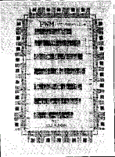
pad frame. The final layout of PWM after the automated placement and routing is shown in Figure 2. The horizontal row
placement of the individual cells is indicative of standard cell designs. |
| The PWM circuit was packaged in a standard 28-pin ceramic DIP by MOSIS. The second design pass provided a100
percent yield of working parts. The PWM circuit performed well up to an input frequency of 18 MHz providing a 36 KHz
IO-bit resolution PWM signal. The device was tested with the PWM amplifiers and microprocessor interface to be used in
the final DAME design and it met all design specifications. Final implementation in 2U SCMOS .A third and final pass was
taken to provide two PWM interfaces in a single chip. This final circuit was implemented in 2-micron SCMOS using the
core design from the previous design effort. In fact, it was the first successful 2-micron design to be fabricated through
MOSIS at the University of Tennessee. The third pass was made to incorporate two identical PWM generators with
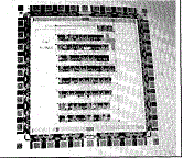
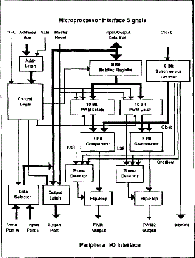
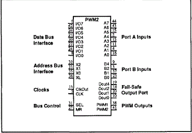
additional parallel digital input output paths. A photograph of the layout of the PWM2 circuit is shown in Figure 3, and a
block diagram of the circuit is shown in Figure 4. The standard cell design layout approach can be seen in Figure 3. The
resulting optimized layout that resulted from applying Turner Wolf SC provided eight horizontal rows of cells. These rows
can be easily identified in the figure. |
PACKAGING |
| The last step in the fabrication of the ASIC integrated circuit is the choice of and requirements for packaging the integrated
circuit. The main factor in the choice of the package for our implementation is the lack of space. The DAME module is
fabricated on a 10.16 centimeter diameter circular printed circuit board so that the resulting manipulator module could be
kept as small as possible. module was also constrained by the length of the wrist module. This length limited the number of
printed circuit boards to three: the joint controller board, the PWM controller interface and optical encoder interface board,
and the 500 watt PWM motor amplifier interface. |
CONCLUSION |
| A brief overview of the design and implementation of an application specific integrated circuit for dual-axis motion control
was presented. The initial design was produced using a personal computer based CAD design program and the layout
design performed on a SUN workstation using VLSI design tools. The integrated circuit was fabricated through the Metal
Oxide Semiconductor Implementation Service (MOSIS) using standard cells implemented in 2- micron Scalable CMOS
(SCMOS) technology. The design and implementation of inexpensive Asics represents a significant milestone in the design
and implementation of the Advanced Tele Robot Manipulator. The project was a success and the ASIC design was
completely functional after the second attempt and has been incorporated in the final design of the Advanced TeleRobot
manipulator control electronics. The ASIC performs the interface between the microprocessor-based joint controller and the
sensor and drive circuit interfaces.. The successful implementation of the PWM ASIC integrated circuit also provides a
great deal of confidence in the ability to utilize VLSI design tools for custom in-house designs and knowledge of the cost
and amount of design effort needed to undertake such a task. |
| |
Figures at a glance |
 |
 |
 |
 |
 |
| Figure 1 |
Figure 2 |
Figure 3 |
Figure 4 |
Figure 5 |
|
| |
References |
- H.L.Martinetal., "Recommendations for the Next- Generation Space TeleRobot System," ORNL Technical Memoranda ORNUTM-9951, April 21, 1986.
- P. E. Satterlee, Jr., H. L. Martin, and R. F. Spille, " Applying the Novix Computer to Real-time Control of Redundant Teleoperator and Robotic Manipulators," U. S. Department of Energy Contract No. DE-ACO5- 86ER80406, January, 1987.
- H. L. Martin, P. E. Satterlee, and R. F. Spille, "Analysis and Design Enhancements for the Advanced Servo manipulator System," U. S. Department of Energy Contract No. DE-AC05-86ER80406, January, 1987.
- H. L. Martin, P. E. Satterlee and W. C. Appleton, âÃâ¬ÃÅDevelopment of Dual-Arm Robotic Manipulator Control Based on Tele operated Manipulation Methods," NASA Contract No. NASI-18423, August, 1987.
- R. R. Kumar, Tennessee, Knoxville, August 1988.
|