Reversible logic is one of the most important issues at present time and it has different areas for its application. The main purposes of designing reversible logic are to decrease quantum cost, depth of the circuits and the number of garbage outputs. A new reversible gate COG is proposed in this paper. This paper also represents an ease implementation of 4 –bit arithmetic circuit for 8 operation by using the reversible COG gate .
Keywords |
| Reversible logic, Basic Reversible Gates, Full adder, Arithmetic Operation ,Garbage , Quantum cost |
INTRODUCTION |
| Energy dissipation is one of the most important factors in electrical circuit designing. Reversible logic was first related
to energy when Landauer states that information loss due to function irreversibility leads to energy dissipation in 1961
who stated that there is small amount of heat dissipation the circuit due to loss of one bit of information and it would be
equal to kTln2 where ‘k’ is Boltzman constant and T is the temperature [1]. This principle is further supported by
Bennett that zero energy dissipation can be achieved only when the circuit contains reversible gates in 1973.It was
proved by Bennett that the energy kTln2 would not be dissipate from the circuit if input can be extracted from output
and it would be possible if and only if reversible gates are used[2]. According to Moore’s law the numbers of
transistors will double every 18 months. Thus energy conservative devices are the need of the day. The amount of
energy dissipated in a system bears a direct relationship to the number of bits erased during computation. Reversible
circuits are those circuits that do not lose information A circuit will be reversible if input vector can be specifically
retrieved from output vectors and here is one to one correspondence between input and output [3]. Younis and Knight
[4] showed that some reversible circuits can be made asymptotically energy-lossless if their delay is allowed to be
arbitrarily large. A reversible logic circuit should have the following features [6]: |
| • Use minimum number of reversible gates. |
| • Use minimum number of garbage outputs. |
| • Use minimum constant inputs. |
LITERATURE SURVEY |
| Landauer, Rolf. [1]." Irreversibility and Heat Generation in the Computing Process". R Landauer’s showed, amount of
heat generation due to loss of bit is kTlog2, and this value is approx 2.8*10-21 joule, which is small but not negligible.
Bennett, Charles H [2]. "Logical Reversibility of Computation". Bennett showed that this heat dissipation due to
information loss can be avoided if the circuit is designed using reversible logic gates. No amount of heat would be
dissipated from the system as long as the system was able to return to its initial state from its final state. E.Fredkin, T
Toffoli, Peres [9] [10] [12] proposed reversible logic gates..In “Optimal Design of a Reversible Full Adder”[18] Yvan
Van Rentergem and Alexis De Vos presented four designs for Reversible full-adder circuits and the implementation of
these logic circuits into electronic circuitry based on CMOS technology and pass-transistor design. In “A General
Method of Constructing the Reversible Full-Adder”[19] Lihui Ni, Zhijin Guan, and Wenying Zhu described general
approach to construct the Reversible full adder and can be extended to a variety of Reversible full adders with only two
Reversible gates. In “Efficient adder circuits based on a conservative reversible logic gate”,[20] Bruce, J.W., M.A.
Thornton, L. shivakuamaraiah, P.S. kokate and X. Li, used only Fredkin gates to construct full adder with gates cost equal to 4, 3 garbage outputs and 2 constant input. In “An Arithmetic Logic Unit Design Based on Reversible Logic
Gates” [5] Zhijin Guan, Wenjuan Li, Weiping Ding, Yueqin Hang, Lihui Ni. Proposed a method for using the
reversible logic gates as logic devices to structure the reversible ALU. In “Design and Analysis of 16 bit reversible
ALU”. Lekshmi Viswanath, Ponni.M [17], presented that circuit designed using reversible logic has reduce delay and
power |
RELATED WORK |
| A. Reversible logic Function |
| It is an n-input n-output logic function in which there is a one-to-one correspondence between the inputs and the
outputs. Because of this bijective mapping the input vector can be uniquely determined from the output vector. This
prevents the loss of information which is the root cause of power dissipation in irreversible logic circuits. The
reversible logic circuits must be constructed under two main constraints. They are |
| • Fan-out is not permitted. |
| • Loops or feedbacks are not permitted |
| The quantum cost(QC) of any reversible gate(circuit) is the number of 1×1 or 2×2 reversible gates and quantum logic
gates such as V, V+ (V is also named square root of NOT gate NOT and V+ is hermitian of V). The V and V+ quantum
gates have some properties that are shown in Equation (1) (Mohammadi et al., 2009). |
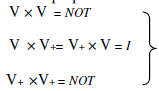 Equation (1) Equation (1) |
| Any reversible logic gate (circuit) is realized by using mentioned gates above, NOT and FG gates. The properties above
show that when two V gates are in series they will behave as a NOT gate. Similarly, two V + gates in series also
function as a NOT gate. A V gate in series with V + gate, and vice versa, is an identity. |
| B. Reversible logic Gates |
| The important basic reversible logic gates are, Feynman gate [7] which is the only 2*2 reversible gate which is as
shown in the figure.1a and it is used most popularly by the designers for fan-out purposes. There is also a double
Feynman gate [8], Fredkin gate [9] and Toffoli gate [10],New Gate[11] , Peres gate[12] , all of which can be used to
realize important combinational functions and all are 3*3 reversible gates and are as shown in the figure.1b to figure.1e
.The figures also shows the switching functions for terminals |
A 4X4 DKFG REVERSIBLE GATE |
| A 4 * 4 reversible gate DKFG already had been proposed [13] shown in figure 2. In this gate the input vector is given
by IV = (0, A, B, C) and the corresponding output vector is OV= (P, Q, R, S). |
| We can implement half-adder by using DKFG gate as shown in fig 2a.We can use DKFG gate as a full-adder as shown
in fig2b |
A NEW PROPOSED 3X3 REVERSIBLE GATE |
| A 3X3 reversible gate COG (Controlled Operation Gate) logic has been proposed in this paper (See Figure 3). The
Truth table for the corresponding gate is shown in figure 3 also .The A closer look at the Truth Table reveals that the
input pattern corresponding to a specific output pattern can be uniquely determined and thereby maintaining that there
is a one-to-one correspondence between the input vector and the output vector. In this gate the input vector is given by
IV = (A, B, C) and the corresponding output vector is OV = (P, Q, R) |
DESIGN OF ARITHMETIC CIRCUIT |
| ALU is a data processing component, which is an important part in centre process unit (CPU). Different kinds of
computers have different ALUs. But all of the ALUs contain arithmetic unit and logic unit, which are the basic
structures. The basic component of the arithmetic section of an ALU is a parallel adder. A parallel adder is constructed
with a number of full adder circuits connected in cascade. By controlling the data inputs to the parallel adder, it is
possible to obtain different types of arithmetic operations. Figure 4 shows the arithmetic operations obtained when one
set of inputs to a parallel adder is controlled externally. |
| The number of bits in the parallel adder may be of any value. The input carry C in goes to the full adder circuit in the
least significant bit position and the C out comes from the full adder circuit in the most significant bit position. From
the figure 4(a) to 4(h) we can see various type of eight operations can be achieved by controlling the B input and
Cin.So to design the circuit we need two parts, one is control circuit and the another one is full adder. |
CONVENTIONAL LOGIC DIAGRAM OF 4 BIT ARITHMETIC CIRCUIT |
| The conventional logic diagram of4 bit arithmetic circuit is shown in figure5.The circuit that controls the input B to
provide various type of operation shown in figure4 consists of two NAND gates, one OR gate and one NOT gate. The
circuit is called a true/complement, one/zero element. There are two selection lines S1and S0 to control the B input.
When S1S0=00 the output of the OR gate Y=0, When S1S0=01 the output of the OR gate Y=B, When S1S0=10 the
output of the OR gate Y=B’and When S1S0=11 the output of the OR gate Y=B+B’=1 |
| From the figure 5we can see that the parallel adder constitutes of four full adder .The carry into the first stage is the
input carry. The carry out of the fourth stage is the output carry. The selection variables are S1,S0 and Cin. Variables
S1S0 control all the B inputs to the full adder circuits. The A inputs go directly to the other inputs of the full adder. The
arithmetic circuit operation is given below in table 1. |
IMPLEMENTATION OF 4 BIT ARITHMETIC CIRCUIT BY REVERSIBLE GATE |
| We can implement one bit arithmetic logic unit by using the proposed reversible COG gate as a control unit shown
in fig 6. .From the truth tables of COG gate [Figure3] we can see that the input B can be controlled depending upon the
value of S1 and S0. |
| We can now implement the four bit arithmetic circuit for eight operations by cascading this four one bit arithmetic
circuit shown in figure 7. But here DKFG reversible gate has been used as a full adder. So we need four DKFG
reversible gates for constructing parallel adder.F3F2F1F0 represents output functions. |
CONCLUSION |
| In this paper, arithmetic unit using reversible control unit COG has been proposed. We have compared these proposed
design with the existing designs [14,16] in terms of reversible gates used, Garbage outputs, constant inputs, &
arithmetic functions. Arithmetic reversible control unit has also great improvement over existing designs [14, 15]. So
the proposed design implementation of reversible ALU in terms of number of gates used, Garbage outputs and
constants input can be used for low power applications. In future we can design complete reversible computer
architecture with the help of proposed designs. The reversible ALU will be a central unit in a future design of a fully
reversible architecture using only reversible logic elements. For a complete architecture, more key elements must be
designed including a reversible control unit and a new approach to reversible memory. |
| |
Tables at a glance |
 |
|
| Table 1 |
Table 2 |
|
| |
Figures at a glance |
 |
 |
 |
 |
| Figure 1 |
Figure 2 |
Figure 3 |
Figure 4 |
 |
 |
 |
| Figure 5 |
Figure 6 |
Figure 7 |
|
| |
References |
- R.Landauer,-Irreversibility and Heat Generation in the Computational Process, IBM Journal of Research and Development, 5, pp. 183-191, 1961 .
- C.H. Bennett, Logical Reversibility of Computation‖, IBM J.Researchand Development, pp. 525-532, November 1973 .
- Pradeepsingla and Naveen kr. Malik “ A Cost - Effective Design of Reversible programmable logic array”International Journal Of Computer Application , volume 41 – no. 15, march- 2012.
- S.Younis and T. Knight, “Asymptotically Zero Energy Split-Level Charge Recovery Logic,”Workshop on Low Power Design, June1994
- Zhijin Guan, Wenjuan Li, Weiping Ding, Yueqin Hang, Lihui Ni “An Arithmetic Logic Unit design based on reversible logic gates”IEEEPacific Rim Conference on Communications, Computers and Signal Processing (PacRim), 2011
- Perkowski, M. and P. Kerntopf, “Reversible Logic. Invited tutorial“ Proc. EURO-MICRO, Warsaw, Poland ,Sept 2001
- R. Feynman, “Quantum Mechanical Computers”,Optical News, pp. 11-20, 1985
- B. Parhami; “Fault Tolerant Reversible Circuits” Proc. 40th AsilomarConf. Signals, Systems, and Computers, Pacific Grove,CA, Oct.2006
- E. Fredkin, T. Toffoli, “Conservative Logic”,International Journal of Theor. Physics, 21, pp.219-253, 1982.
- T. Toffoli., “Reversible Computing”, Tech memo MIT/LCS/TM‐151,MIT Lab for Computer Science (1980).
- Md. M. H Azad Khan, “Design of Full-adder With Reversible Gates”, International Conference on Computerand Information Technology, Dhaka, Bangladesh,pp.515-519,2002
- Peres, A.. Reversible logic and quantum computers, Physical Review: A, 32 (6): 3266-3276, 1985
- Shefali Mamataj1,Biswajit Das2, Anurima Rahaman3 “An Approach for Realization of 2’s Complement Adder SubtractorUsing DKG Reversible gate ‘, International Journal of Emerging Technology and Advanced Engineering: Volume 3, Issue 12, December 2013)
- ZhijinGuan,WenjuanLi,WeipingDing,YueqinHang,andLihui Ni, “An Arithmetic Logic Unit Design Based on Reversible Logic Gates”,Communictions ,Computers and Signal Processing (PacRim)v , pp.925-931, 03 October 2011
- Akanksha Dixit, “VinodKapse,Arithmetic& Logic Unit (ALU) Design using Reversible Control Unit” International Journal of Engineering and Innovative Technology (IJEIT) Volume 1, Issue 6, June 2012
- Y. Syamala, and A. V. N. Tilak, “Reversible Arithmetic Logic Unit”, Electronics Computer Technology (ICECT), 2011 3rd International, vol. 5, pp.207-211,07 july 2011.
- LekshmiViswanath,Ponni.M’ ‘Design and analysis of 16 bit reversible ALU”, IOSR Journal of Computer Engineering (IOSRJCE) ISSN : 2278-0661 Volume 1, Issue 1, PP 46-53, (May-June) 2012
- Yvan Van Rentergem and Alexis De Vos, ―Optimal Design of a Reversible Full Adder‖, International Journal of Unconventional Computing, vol. 1, pp. 339 – 355, 2005
- 19 Lihui Ni, Zhijin Guan, and WenyingZhu,A General Method of Constructing the Reversible Full-Adder, Third International Symposium on Intelligent Information Technology and Security Informatics, pp.109-113, 2010
- 20 Bruce, J.W., M.A. Thornton, L. shivakuamaraiah, P.S. kokate and X. Li-Efficient adder circuits based on a conservative reversible logic gate‖, IEEE computer society Annual symposium on VLSI, Pittsburgh, Pennsylvania, and pp: 83-88, 2000
|