International Journal of Advanced Research in Electrical, Electronics and Instrumentation Engineering
ISSN ONLINE(2278-8875) PRINT (2320-3765)
ISSN ONLINE(2278-8875) PRINT (2320-3765)
|
P.Premkumar and S.Nandhini Assistant professor, Dept. of ECE, Nandha Engineering College, Erode, Tamilnadu, India |
| Related article at Pubmed, Scholar Google |
Visit for more related articles at International Journal of Advanced Research in Electrical, Electronics and Instrumentation Engineering
A static CMOS inverter does not dissipate power during the absence of transients on the input. During a transient in the input, there will be a time period in which both the NMOS Transistor and PMOS Transistor will conduct, causing a short circuit to flow from supply to ground for an inverter without load. For a CMOS circuit, the total power dissipation, includes dynamic and static components during the active mode of operation. To overcome the drawback of Complementary inverter, the ULV inverters are used in the design. The dynamic power consumption is reduced significantly with reduced supply voltage. The static power consumption is more dependent on the transistor threshold voltage. Scaling the supply voltage and threshold voltage reduces the dynamic power dissipation and static power dissipation respectively. In order to achieve high performance for low power consideration, the threshold voltage is scaled along with the supply voltage. The power consumption depends on the recharge voltage and the supply voltage. Therefore optimizing the supply voltage and recharge voltage results in reduced power consumption. Ultra Low Voltage Low Power CMOS Inverter the offset voltage is scaled along with the threshold voltage. The Ultra Low Voltage Inverter is configured to low power compared to that compared to that of a complementary inverter. A complementary inverter is designed using Tanner EDA Tool. The complementary inverter is used as the basic module for the design of the full adder. The power consumed by the full adder which is designed using the complementary inverter is calculated. Similarly, the Ultra Low Voltage Inverter is designed by Tanner EDA Tool. The Ultra Low Voltage Inverter is used as the basic module for the design of the full adder. The power consumed by the full adder which is designed using the Ultra Low Voltage Inverter is calculated. The objective is to prove that the power consumed by the Ultra Low Voltage Inverter is lower than that of the complementary inverter. Thus, the Ultra Low Voltage Inverter is configured to operate at low power compared to that of the complementary inverter. The logos presented here are designed for the 90nm process using Tanner EDA Tool.
Keywords |
||||||||||||||
| Ultra low voltage CMOS, Power dissipation, Inverter, Adder. | ||||||||||||||
INTRODUCTION |
||||||||||||||
| The most fundamental and effective approach to reduce power consumption in CMOS logic is to lower the supply voltage. For a CMOS circuit, the total power dissipation, includes dynamic and static components during the active mode of operation. The dynamic power consumption is reduced significantly with reduced supply voltage. The static power consumption is more dependent on the transistor threshold voltage. However, scaling the supply voltage has an adverse effect on the performance of the circuit, i.e. it could lead to a severe penalty in circuit speed. Power savings can also be achieved by a number of architectural solutions. In order to achieve high performance for low power consideration, the threshold voltage is scaled along with the supply voltage [8]. The power consumption depends on the recharge voltage and the supply voltage. Therefore optimizing the supply voltage and recharge voltage results in reduced power consumption. For high performance, low power consideration, the device threshold voltage is scaled lowering the supply-voltage. | ||||||||||||||
| However, in modern CMOS technologies, there are significant gate leakages. ULV gates implemented in a modern CMOS process require frequent initialization to avoid significant leakage. There are several approaches to CMOS logic. The gates proposed in this paper are influenced by ULV and recharge logic. It is evident that methodologies for the design of high-throughput, low-power digital systems are needed. Fortunately, there are clear technological trends that give us a new degree of freedom, so that it may be possible to satisfy these seemingly contradictory requirements. | ||||||||||||||
| Scaling of device feature sizes, along with the development of high-density, low-parasitic packaging, such as multichip modules, will alleviate the overriding concern with the numbers of transistors being used. When MOS technology has scaled to 0.2-μm minimum feature size, it will be possible to place from 1 to 10 X 109 transistors in an area of 8 inch X 10 inch if a high-density packaging technology is used [5]. | ||||||||||||||
RELATED WORKS |
||||||||||||||
| A.T.Schwarzbacher [1] presented a novel on “Benchmarking CMOS adder structures”. Adders are key components in digital signal processing, performing not only addition operations, but also many other functions such as subtraction, multiplication and division. | ||||||||||||||
| Chip-Hong Chang [2] presented a novel on “ A review of 0.18μm full adder performances for tree structured arithmetic circuits”.The general objective of the work is to investigate the area and power-delay performances of low-voltage full adder cells in different CMOS logic styles for the predominating tree structured arithmetic circuits. David Levacq [3] presented a novel on “Low leakage SOI CMOS static memory cell with ultra-low power diode”. A new CMOS digital storage device is developed based on the combination of two reverse biased composite CMOS diodes, each of them featuring ultra-low leakage and a negative impedance characteristic in reverse mode. | ||||||||||||||
| Dhireesha Kudithipudi [4] presented a novel on “Implementation of low power digital multipliers using 10 transistor adder blocks”. The increasing demand for the high fidelity portable devices has laid emphasis on the development of low power and high performance systems. The low power design has to be incorporated into fundamental computation units, such as multipliers. | ||||||||||||||
| Jyh-Ming Wang [5] presented a novel on “New efficient designs for XOR and XNOR functions on the transistor level”. Two new methods are to implement the exclusive-OR and exclusive-NOR functions on the transistor level. The first method uses non-complementary signal inputs and the least number of transistors. The other one improves the performance of the prior method but two more transistors are utilized. The latter uses the same number of transistors but with more driving capability additionally. | ||||||||||||||
| Richard X. Go [8] presented a novel on “Power dissipation analysis and optimization of deep submicron CMOS digital circuits”.A Simple analytical model for estimating stand by and switching power dissipation in deep submicron CMOS digital circuits. The model is based on Berkeley Short-Channel IGFET model and fits HSPICE simulation results well. Sumeer Goel [9] presented a Novel on “Design of robust, energy-efficient full adders for deep-sub micrometer design using hybrid-cmos logic style”. A new design for a 1-bit full adder featuring hybrid-CMOS design style. The quest to achieve a good-drivability, noise-robustness, and low-energy operations for deep sub micrometer guided our research to explore hybrid-CMOS style design. | ||||||||||||||
SOURCES OF POWER DISSIPATION |
||||||||||||||
| There are three major sources of power dissipation in digital CMOS circuits, which are summarized in the following equation: | ||||||||||||||
| The first term represents the switching component of power, where CL is the load capacitance, fclk is the clock frequency, Ileakage is the leakage current, Ptotal is the total power dissipation, Isc is the short circuit current, VDD is the supply voltage and Pt is the probability that a power consuming transition occurs (the activity factor). In most cases, the voltage swing is the same as the supply voltage. The second term is due to the direct-path short circuit current, which arises when both the NMOS and PMOS transistors are simultaneously active, conducting current directly from supply to ground [5]. Finally, leakage current Ileakage, which can arise from substrate injection and sub threshold effects, is primarily determined by fabrication technology considerations. The power-delay product can be interpreted as the amount of energy expended in each switching event and is thus particularly useful in comparing the power dissipation of various circuit styles. | ||||||||||||||
| DESIGN ISSUES FOR LOW VOLTAGE CMOS CIRCUITS | ||||||||||||||
| Low voltage operation | ||||||||||||||
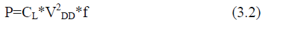
| Power dissipation in digital circuit is expressed as | ||||||||||||||
 |
||||||||||||||
| Where CL is the load capacitance, VDD is the supply voltage and f is the operating frequency. According to this formula, lowering VDD is the most effective way to reduce power dissipation because it is proportional to the square of VDD [1]. | ||||||||||||||
| Figure 3.2 shows the relation between power consumption and supply voltage. It is apparent that lowering VDD contributes to power reduction. Certainly, scaling down load capacitance or operating frequency also contributes to low-power operation. Decreasing capacitance CL, however, would be difficult without scaling down the device and wiring. Although there have been attempts to lower operating frequency by introducing parallel processing, this approach generally increases hardware overhead and requires extensive reworking at an architecture or algorithm design level. | ||||||||||||||
| Key issue for low voltage operation | ||||||||||||||
| In CMOS digital circuits, the gate delay time (tpd) is approximately given by | ||||||||||||||
| Where CL is the load capacitance, IDS is the drain current in the saturation region, VDD is the supply voltage, Vth is the MOSFET threshold voltage, and A is a constant. In the above expression, lowering the supply voltage decreases IDS proportional to the square of the voltage difference (VDD–Vth). Supply voltage is lowered by scaling down the device feature size to ensure the reliability of thin gate oxides. Speed performance is maintained even at low voltage due to the improvement in transconductance gm brought about by shrinking feature size to a deep submicron size. In this case, a decrease in delay time at lower voltage must be achieved without relying on device feature size scaling. One way to overcome the speed degradation problem is to reduce the Vth of a MOSFET [1]. | ||||||||||||||
CIRCUIT DESIGN AND TECHNOLOGY CONSIDERATIONS |
||||||||||||||
| Threshold voltage scaling | ||||||||||||||
| A significant power improvement can be gained through the use of low threshold MOS devices; the question of how low the thresholds can be reduced must be addressed. The limit is set by the requirement to retain adequate noise margins and the increase in sub threshold currents. Noise margins will be relaxed in low-power designs because of the reduced currents being switched, however, the sub threshold currents can result in significant static power dissipation. Essentially, sub threshold leakage occurs due to carrier diffusion between the source and the drain when the gate-source voltage, has exceeded the weak inversion point, but is still below the threshold voltage, where carrier drift is dominant. In this region, the MOSFET behaves similarly to a bipolar transistor and the sub threshold current is exponentially dependent on the gate-source voltage and approximately independent of the drain-source voltage for Vds approximately larger than 0.1 V. Associated with this is the sub threshold slope, which is the amount of voltage required to drop the sub threshold current by one decade [1]. | ||||||||||||||
| For a CMOS inverter (PMOS: W = 8pm, NMOS: W = 4 pm) the current was measured to be 64 mA over 3.7 ns at a supply voltage of 2 V. This implies that there would be a 100% power penalty for sub threshold leakage if the device were operating at a clock speed of 25 MHz with an activity factor of p = 1 /6th, i.e., the devices were left idle and leaking current 83 % of the time. It is not advisable, therefore, to use a true zero threshold device, but instead to use thresholds of at least 0.2 V, which provides for at least two orders of magnitude of reduction of sub threshold current. This provides a good compromise between improvement of current drive at low supply voltage operation and keeping sub threshold power dissipation to a negligible level. This value may have to be higher in dynamic circuits to prevent accidental discharge during the evaluation phase. Fortunately, device technologists are addressing the problem of sub threshold currents in future scaled technologies and reducing the supply voltages also serves to reduce the current by reducing the maximum allowable drain-source voltage. The design of future circuits for lowest power operation should therefore explicitly take into account the effect of sub threshold current [5]. | ||||||||||||||
| Voltage scaling | ||||||||||||||
| The reduction of supply voltage should yield even greater benefits. Reducing the supply voltage is the key to lowpower operation, even after taking into account the modifications to the system architecture, which is required to maintain the computational throughput. First, a review of circuit behavior (delay and energy characteristics) as a function of scaling supply voltage and feature sizes will be presented. By comparison with experimental data, it is found that simple first-order theory yields an amazingly accurate representation of the various dependencies over a wide variety of circuit styles and architectures. A survey of two previous approaches to supply- voltage scaling is then presented, which were focused on maintaining reliability and performance. This is followed by our architecture-driven approach, from which an “optimal” supply voltage based on technology, architecture and noise margin constraints is derived. | ||||||||||||||
| Optimal transistor sizing with voltage scaling | ||||||||||||||
| Independent of the choice of logic family or topology, optimized transistor sizing will play an important role in reducing power consumption. For low power, it is important to equalize all delay paths so that a single critical path does not unnecessarily limit the performance of the entire circuit. However, beyond this constraint, there is the issue of what extent the W/L ratios should be uniformly raised for all the devices, yielding a uniform decrease in the gate delay and hence allowing for a corresponding reduction in voltage and power. It is shown in this section that if voltage is allowed to vary, that the optimal sizing for low-power operation is quite different from that required for high speed [7]. | ||||||||||||||
| Optimal supply voltage | ||||||||||||||
| In the previous section, the delay increases due to reduced supply voltages below the critical voltage and can be compensated by exploiting parallel architectures. However, as supply voltages approach the device thresholds, the gate delays increase rapidly[6]. Correspondingly, the amount of parallelism and overhead circuitry increases to a point where the added overhead dominates any gains in power reduction from further voltage reduction, leading to the existence of an “optimal” voltage from an architectural point of view. | ||||||||||||||
| At very low supply voltages (near the device thresholds), the number of processors (and hence the corresponding overhead in the above equation) typically increases at a faster rate resulting in a power increase with further reduction in voltage. Reduced threshold devices tend to lower the optimal voltage. At threshold below 0.2 V, power dissipation due to the sub threshold current will soon start to dominate and limit further power improvement. An even lower bound on the power supply voltage for a CMOS inverter with “correct” functionality was found to be 0.2 V. There are a variety of considerations that must be taken into account in low-power design which include the style of logic, the technology used and the logic implemented. Factors that were shown to contribute to power dissipation included spurious transitions due to hazards and critical race conditions, leakage and direct path currents, pre-charge transitions, and power-consuming transitions in unused circuitry [5]. | ||||||||||||||
ULTRA LOW VOLTAGE CMOS GATE |
||||||||||||||
| The Ultra Low Voltage CMOS logic is shown in Fig.5.1. The biasing or recharge transistors, marked Rp and Rn are used to set the voltage level during initialization. | ||||||||||||||
| When the circuit is initialized or recharged two tasks are performed in parallel: | ||||||||||||||
| 1) The Ultra low voltage gates are biased or recharged through the biasing transistors. The NMOS Gates is biased to VDD and the PMOS Gate is biased to VSS. The clock drivers provide virtual references to the ULV inverter. | ||||||||||||||
| 2) The output is pre-charged to VDD/2. The time constant for the output pre-charge is much larger than the time constant for biasing the nodes. The inverter is reverse biased with a high impedance output. The output transistors En and Ep pull the output towards VDD/2. The output voltage will depend on the previous voltage or logical level and on the time available in the initialization phase. The logic operation of the gate is not depending on the accuracy of the output pre-charge value [3]. | ||||||||||||||
| When the gate is recharged, the PMOS will initially operate in strong inversion due to an effective voltage Veff = VG−VS−VT ≈ (5/4)VDD−VT . When the reference voltages starts the transition to reverse biased mode the output of the gate (ULV) will be at a potential below both references, hence the transistor currents through Ep and En will be positive seen from the output and thus pull the output quickly towards VDD/2. If the output is equal to VDD at the start of the recharge period, due to a negative input transition, both output transistors En and Ep will contribute pulling the output quickly towards VDD/2. The biasing delay for the output is larger because the output transistors are reverse biased and the output impedance is low. Preliminary data suggest that a ULV inverter is able to respond correctly to a input transition less than 40 mV [4]. The gate drain capacitance will degrade the performance through a reduced Tranconductance and gain. Transistor mismatches, i.e. threshold voltage variations, will also affect the recharge output value of the ULV gate. If the NMOS Gate, En is strong compared to Ep the output recharge level will settle at a voltage higher than VDD/2 [3]. | ||||||||||||||
| The ULV gate operation is characterized by: | ||||||||||||||
| • Recharge. The simplified ULV inverter in recharge mode is shown in Figure 5.2 (a). The NMOS Gate is recharged to V+ and the PMOS Gate is recharged to V− while the output and input are precharged to VDD/2. The output will be forced to VDD/2 due to a reversed biased inverter. | ||||||||||||||
| • Evaluate. The simplified ULV inverter in evaluate mode is shown in Figure 5.2 (b). The output will be pulled to VDD/2 if a negative transition ΔVin = −VDD/2 occurs and to GND if there is a positive transition ΔVin = VDD/2, applied at the input. | ||||||||||||||
| The PMOS Clocked transistor is obtained using a PMOS evaluate transistor and a NMOS recharge transistor. The clock drivers which provide both the control signals and the reference signals in the evaluation phase is included. The effective supply voltage is determined by the clock signal φ and the recharge voltages V+ and V− regulate the current level. The ULV logic style resembles domino logic [8]. The output of the ULV gate will always be driven and less susceptible to noise than dynamic domino logic. The ULV inverter in recharge and evaluate mode is shown in Figure 5.2. | ||||||||||||||
| A low voltage and high speed configuration is achieved if a high offset voltage V+ and V− = VDD−V+ is applied. The ULV inverter will not be recharged as fast as the low voltage and high speed ULV inverter due to the reduced currents running through the recharge transistors. Both the evaluate response and the recharge response will be slower together with the dynamic and static power consumption. The recharge current is determined by a effective bias of the recharge transistors. The accuracy of the pre-charge level is not significant for an inverter gate, however if more complex gates with higher fan-in is required the pre-charge level need to be close to VDD/2. | ||||||||||||||
RESULTS AND DISCUSSION |
||||||||||||||
| Design of half adder usingUltra low voltage inverter | ||||||||||||||
| Figure 6.1 shows the schematic diagram of half adder using ultra low voltage inverter. It shows that the power consumed by the design is very low when compared with the complementary inverter. The Ultra low voltage gates are biased or recharged through the biasing transistors. The time constant for the output pre-charge is much larger than the time constant for biasing the nodes. | ||||||||||||||
| Figure 6.2 shows the output waveform of half adder using ultra low voltage inverter. The waveform shows the functionality of the half adder. The circuit is designed and simulated in tanner tool. | ||||||||||||||
| It has been found that the power consumed by a half adder using complementary inverter in Tanner EDA Tool was 3.460128e-005 and the power consumed by the half adder using Ultra low voltage inverter was 7.301789e-007. | ||||||||||||||
| Design of Full adder using Ultra low voltage inverter | ||||||||||||||
| Figure 6.3 shows the schematic diagram of full adder designed using ultra low voltage inverter. It is constructed using two half adders those which are designed using ultra CMOS logic. The Circuit designed is of low voltage and power consumed is extremely low. | ||||||||||||||
| Figure 6.4 shows the output waveform for the corresponding input waveform. It shows the functionality of full adder. It has been found that the power consumed by a Full adder gate using complementary inverter in Tanner EDA Tool was 5.334652 e-004 and the power consumed by the Full adder using Ultra low voltage inverter was 2.84582e-004. | ||||||||||||||
CONCLUSION |
||||||||||||||
| The performance of the ultra low voltage (ULV) logic style is compared to a complementary inverter. The complementary inverter is designed using Tanner EDA Tool and its power consumption is measured. The total power dissipation which is the combination of static power dissipation and dynamic power dissipation is reduced by scaling the threshold voltage along with the supply voltage. This complementary inverter is used as the basic module for the design of the full adder and its power consumption is measured. Similarly, the Ultra Low Voltage Inverter is designed using Tanner EDA Tool and its power consumption is measured. It is proved that the power consumed by the Ultra Low Voltage Inverter is low compared to that of the complementary inverter. This shows that the use of the Ultra Low Voltage Inverter as a basic module in any design would result in low power consumption compared to that of a complementary inverter. The ULV logic gates can be utilized to design fast systems operating at ultra low supply voltages. The simulated data presented is obtained using the Tanner EDA Tool and executed for a 90nm CMOS process. The dynamic power consumption is reduced significantly with reduced supply voltage. Thus the Ultra Low Voltage Inverter is configured to operate at low power compared to that of a complementary inverter. | ||||||||||||||
Figures at a glance |
||||||||||||||
|
||||||||||||||
References |
||||||||||||||
|


