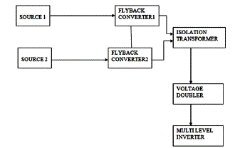
There is an increasing demand of power and load shedding is preferred as a solution. An interruption for a few cycles of power supply results in loss of data, mal functioning of various sensitive equipments. A model is developed to provide uninterrupted power supply to the consumers in the event of failure of the main input source. The different modes of operation that has been developed are normal, back-up and charging. The output of the integrated flyback converter is given to the multilevel inverter. A cascaded H-bridge multilevel inverter is implemented using a single DC power source and capacitors. A standard cascaded multilevel inverter requires ‘n’ DC sources for ‘2n + 1’ levels. Without requiring transformers, the scheme proposed allows the use of a single DC power source (e.g., a battery, a fuel cell stack or photo voltaic panel) with the remaining n−1 DC sources being capacitors. The DC voltage level of the capacitors can be maintained simultaneously and a fundamental frequency switching pattern can be chosen to produce a nearly sinusoidal output. The number of levels is increased up to fifteen by adding six bidirectional switches to a H-bridge inverter. The main objectives are to improve the power quality by reducing the total harmonic distortion to a very low value and the reduction of the per unit cost of electricity.
Keywords |
| Multilevel inverter, flyback converter, Hbridge
configuration, energy storage and management |
INTRODUCTION |
| Now-a-days, we can hardly imagine the lifestyle without
the provision and processing activities which use
electrical energy, and its supply. In recent years, a lot of research has been carried out on the design of
uninterruptible power supply systems to provide clean
and uninterruptible power to equipment in critical
applications under normal or abnormal utility power
conditions for which batteries or flywheels are
incorporated in the UPS for this purpose. The power
conversion is mainly accomplished using power
electronics switches due to the advanced development of
fast-switching and high current capabilities. [1]. A dc
UPS is designed with high efficiency due to single
voltage conversion. The system cost will also be reduced
substantially due to removal of the redundant inverter
and rectifier. It will have small size, which is slightly
larger than a conventional switching power supply but
much smaller than a UPS. So for only a few designs of
such high frequency dc UPS had been reported in [2,3].
All these designs have a common feature that a single
power transistor is used for current switching in both
normal and backup operations, while another transistor is
used for battery charging. While this feature enables full
utilization of the power transistor, the conversion
efficiency in backup operation will be unacceptably low
so we are proposing an integrated fly back converter for
dc UPS application .The proposed converter accepts a
high voltage main input and a low voltage backup battery
input. With separated converter circuits for the main and
battery inputs, the ratings of each switching device can
be optimally selected, thus enabling the converter to
achieve high conversion efficiency in normal, backup,
and charging operations. |
| A cascade multilevel inverter is a power
electronic device built to synthesize a desired AC voltage
from several levels of DC voltages. Such inverters have been the subject of research in the last several years [4]
[5] [6] [7] [8], where the DC levels are considered to be
identical and all of them were either batteries, solar cells
or any other source. The advantages are waveforms with
high power quality can be obtained, devices of low
voltage rating can be used, low harmonic distortion, low
switching frequency and switching losses, higher
efficiency, reduction of dv/dt stresses etc. The popular
MLI topologies are Diode Clamp, Flying Capacitor and
Cascaded Multilevel Inverter (CMLI). In this paper we
are using a CMLI that consist of an H-Bridge inverter. In
[8], a multilevel converter was presented in which the
two separate DC sources were the secondary windings of
the two transformers are coupled to the utility AC power.
In contrast, only one source is used without the use of
transformers. A single DC power source is interfaced
with a cascaded multilevel inverter where the other DC
sources are capacitors. Currently, each phase of a
cascade multilevel inverter requires n DC sources for
2n+1 levels in applications that involve real power
transfer. Here, a scheme is proposed that allows the use
of a single DC power source (e.g., battery or fuel cell
stack) with the remaining n − 1 DC sources being
capacitors. It is shown that one can simultaneously
maintain the DC voltage level of the capacitors and
choose a fundamental frequency switching pattern to
produce a nearly sinusoidal output. |
INTEGRATED FLY BACK CONVERTER |
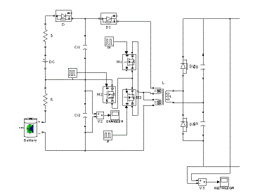
| The circuit of the proposed integrated fly back converter
is shown in Fig.1. |
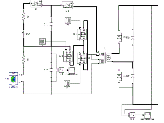
| The switch SW1 is used to select the mode of operation.
When the main power input VAC is functioning
properly, the switch SW1 will be closed and MOSFET
Q2 turned off to operate the converter in normal mode.
The equivalent circuit of the converter in normal mode is
shown in Fig. 2. The battery voltage VB should be
chosen to be higher than Vc1n2/n1 to prevent diode D2
from conducting when Q1 is turned on. Such choice will
make the backup converter (VB, Q2, D2 and n2) idle,
thus disconnecting it from the equivalent circuit during
normal-mode operation. |
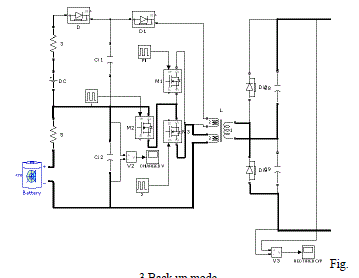
| When input power failure is detected, MOSFET Q1 will
be switched off and switch SW1 will be closed to operate
the converter in backup mode. The equivalent circuit of
the converter in backup mode is shown in Fig.3. |
| As the battery voltage VB is much lower than main
input voltage VCl, the switch current iQ2 in backup will
be much higher than the switch current iQ1 in mode
normal mode. Therefore a low-voltage, low-RDs (on)
MOSFET should be chosen for Q2. The number of turn’s
n2 in the primary of backup converter should be chosen
to be much smaller than n1 in the main converter and
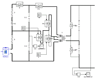
with much higher current winding used. When the main
power input VAC is functioning properly, SW1 can be
opened to operate the converter in the charging mode.
The equivalent circuit of the converter in the charging
mode is another flyback converter as shown in Fig.4. |
| As the battery VB is in series with the main input VCl,
the battery charging current -IB will be equal to the
averaged input current IQ1 from VCl. A disadvantage of
the proposed converter is that the charging current is
load-dependent and cannot be controlled independently.
The converter thus cannot provide battery charging when
there is no load. Battery charging is instead controlled by
charging time, i.e. the duration the converter operates in
charging mode. |
MULTILEVEL INVERTER ARCHITECTURE |
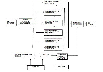
| To operate a cascade multilevel inverter using a single
DC source, it is proposed to use capacitors as the DC
sources for all but the first source. The multi level
inverter comprises of a single-phase conventional Hbridge
inverter, six bidirectional switches, and a
capacitor voltage divider formed by C1, C2, C3, C4, C5,
C6, C7.The H-bridge topology is significantly
advantageous over other topologies, i.e., less power
switches, power diodes, and less capacitor for inverters
of the same number of levels.It generates an almost
sinusoidal waveform voltage while switching only one
time per fundamental cycle. The output voltage
waveform of a multilevel inverter is composed of the
number of levels of voltages, typically obtained from
capacitor voltage sources. The so-called multilevel
inverter starts from three levels. As the number of levels
reach infinity, the output THD approaches zero. The
number of the achievable voltage levels, however, is
limited by voltage imbalance problems, voltage clamping
requirement, circuit layout, and packaging constraints.
When analyzed we arrived at fifteen modes of operation
for the multilevel inverter. |
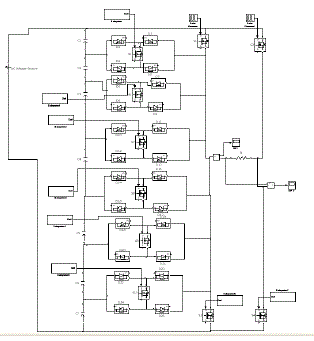
| In case of mode 0 operation the switches S3&S4 are
turned on and capacitors C1-C7 are charged. In mode
1(Vdc/7) operation switches S10&S4 and capacitors C1-
C6 are charged. In mode 2(2Vdc/7) operation switches S9&S4 on capacitors C1-C5 are charged. In mode 3
(3Vdc/7) operation, switches S8&S4 are turned on and
capacitors C1-C4 are charged. In mode 4 (4Vdc/7)
operation, switches S7&S4 are turned on and capacitors
C1, C2 and C3 are charged. In mode 5 (5Vdc/7)
operation, switches S6&S4 are turned on and capacitors
C1 and C2 are charged. In mode 6 (6Vdc/7) operation,
switches S5&S4 are turned on and capacitor C1 is
charged. In mode 7(Vdc) operation switches S1&S4 are
turned on. In mode 8(-6Vdc/7) operation, switches
S10&S2 are turned on and capacitor C7 is charged. In
mode 9(-5Vdc/7) operation, switches S9&S2 are turned
on and capacitors C7 and C6 are charged. In mode 10(-
4Vdc/7) operation, switches S8&S2 are turned on and
capacitors C7, C6 and C5 are charged. In mode 11(-
3Vdc/7) operation, switches S7&S2 are turned on and
capacitors C7, C6, C5 and C4 are charged. In mode 12(-
2Vdc/7) operation, switches S6&S2 are turned on and
capacitors C7-C3 are charged. In mode 13(-Vdc/7)
operation, switches S5&S2 are turned on and capacitors
C7-C2 are charged. In mode 14(-Vdc) operation, switches
S2&S3 are turned on. The duration and the number of
gate pulses are calculated and supplied accordingly. |
SIMULINK MODEL OF THE PROPOSED
CIRCUIT DIAGRAM |
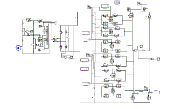
| The simulation has been done with the help of Simulink
in Matlab. |
SIMULATION RESULTS AND DISCUSSION |
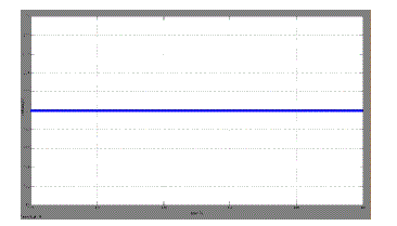
| The fig. 9 shows the simulated input voltage which is
supplied by the renewable energy source |
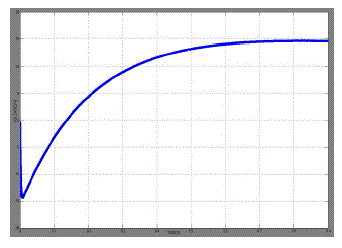
| The fig 10 shows the simulated voltage across the
capacitor connected in parallel to the battery (auxiliary
source) |
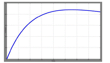
| The fig 11 shows the simulated output of the voltage
doubler which is the input to the multilevel inverter. |
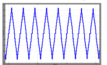
| Fig. 12 shows the simulated output voltage of the fifteen
level inverter. |
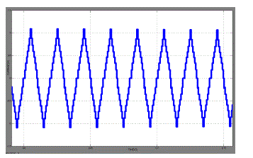
| The fig13 shows that the simulated 15 level output
current for the proposed circuit. |
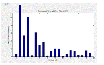
| The harmonic analysis was simulated and was found to
be 16.35%. The fig. 14 shows that the simulated THD of
output current for the proposed circuit. |
CONCLUSION |
| The operation and design of an integrated flyback
converter is explained in detail. The converter features a
simple circuit with high efficiency, small size, and low
cost when compared to the conventional switching power
supply. A cascade multilevel inverter topology has been
proposed that requires only a single DC power source.
The objectives of the proposed method are
harmonic reduction, high efficiency, less isolation and
balanced voltage transfer. The applications include AC
drives, Static var compensator and satellite power
supplies. |
| |
Figures at a glance |
 |
 |
 |
 |
 |
| Figure 1 |
Figure 2 |
Figure 3 |
Figure 4 |
Figure 5 |
 |
 |
 |
 |
 |
| Figure 6 |
Figure 7 |
Figure 8 |
Figure 9 |
Figure 10 |
 |
 |
 |
 |
| Figure 11 |
Figure 12 |
Figure 13 |
Figure 14 |
|
| |
References |
- P. Hunter, âÃâ¬ÃÅBattery backed switcher provides UPS capability,âÃâ¬Ã power conversion and Intelligent Motion. Oct. 1989, pp. 56-59
- P. W. Clarke, âÃâ¬ÃÅReserve battery back-up (RBB) systems employing current-mode feedback for wide bandwidth and large dynamic response,âÃâ¬Ã in Proc. PCZ, Intertec Int., Inc., Apr. 1984, pp. 34-51.
- K.-W. Ma and Y.s. Lee, âÃâ¬ÃÅA novel uninterruptible dc-dc converter for UPS applications,âÃâ¬Ã IEEE Trans. Industry Application, vol. 28, no. 4, pp. 808- 815, July/Aug. 1991.
- M. Klabunde, Y. Zhao, and T. A. Lipo, âÃâ¬ÃÅCurrent control of a 3 level rectifier/inverter drive system,âÃâ¬Ã in Conference Record 1994 IEEE IAS Annual Meeting, 1994, pp. 2348âÃâ¬Ãâ2356.
- W. Menzies, P. Steimer, and J. K. Steinke, âÃâ¬ÃÅFive-level GTO inverters for large induction motor drives,âÃâ¬Ã IEEE Transactions on Industry Applications, vol. 30, no. 4, pp. 938âÃâ¬Ãâ944, July 1994.
- G. Sinha and T. A. Lipo, âÃâ¬ÃÅA four level rectifier-inverter system for drive applications,âÃâ¬Ã in Conference Record IEEE IAS Annual Meeting, October 1996, pp. 980âÃâ¬Ãâ987.
- J. K. Steinke, âÃâ¬ÃÅControl strategy for a three phase AC traction drive with three level GTO PWM inverter,âÃâ¬Ã in IEEE Power Electronic Specialist Conference (PESC), 1988, pp. 431âÃâ¬Ãâ438.
- J. Zhang, âÃâ¬ÃÅHigh performance control of a three level IGBT inverter fed AC drive,âÃâ¬Ã in Conf. Rec. IEEE IAS Annual Meeting, 1995, pp. 22âÃâ¬Ãâ 28.
- M. Manjrekar, P. K. Steimer, and T. Lipo, âÃâ¬ÃÅHybrid multilevel power conversion system: A competitive solution for high-power applications,âÃâ¬Ã IEEE Transactions on Industry Applications, vol. 36, no. 3, pp. 834âÃâ¬Ãâ841, May/June 2000.
|