An improved RF?dc converter based on a class-E rectifier with wide-dynamic-range input matching is presented. The input impedance is controlled by two varactor diodes to compensate for impedance changes with RF input power and dc loading conditions. The RF?dc converter achieved a peak efficiency of 60% and an S11 less than −20 dB over an input RF power range of 12 dB and an operating battery voltage of 2.5?4.2 V at 800 MHz. An analytical model for input impedance and efficiency was developed and shown to match simulation and measurement results.
Keywords |
| Class-E rectifier, hybrid transformer duplexer,impedance matching, power recycling, RF–dc
converter, Schottky diode, Varactor diode. |
| |
INTRODUCTION |
| Numerous technologies use high frequency (HF) electromagnetic fields: Everyday life cannot be
imagined without broadcasting and television, cordless phones increase comfort when phoning indoors and in the
garden, babies are monitored in their rooms using baby monitors, computers are linked to each other and to peripheral
devices by using Wireless LAN (WLAN) and Bluetooth and recently ultra wideband (UWB) technologies, police and
fire brigades use their own radio network for communication. Moreover high frequency fields are applied for radar
units, in microwave ovens and for electronic article surveillance systems. At present new applications for high
frequency fields in the terahertz range are developed and tested (e.g., security scans at airports). The strongest increase
in use, however, has been stated in mobile telecommunication for some years. UMTS and WiMAX technology for fast
data transmission will further increase the frequency of utilisation. Highfrequency (HF) is the ITU-designated range
of radio frequency electromagnetic waves (radio waves) between 3 and 30 MHz.Also known as the decameter
band or decameter wave as the wavelengths range from one to ten decameters (ten to one hundred metres). |
| Manyhigh-frequency applications require a highefficiencyrectifier with a well-behaved input
impedance. Unfortunately, due to the highly nonlinear nature of the rectification process, the input impedance of a
rectifier depends on the input power and loading conditions, which causes degradation in the overall performance when
power and loading change from the nominal design values. |
| One potential application, which is very sensitive to rectifier input impedance, is power recycling in a hybridtransformer
based duplexer. Hybrid transformers have been proposed to replace discrete banks of duplexers due to the
advantages of integration and tenability. However, approximately 50% of the transmit power is lost in the balancing
load. In this brief, we propose an RF–dc converter that recycles the power lost in the balance load while maintaining
the required constant input impedance over a wide range of input power to achieve the desired transmit-to-receive port isolation. Fig. 1 illustrates the hybrid transformer with the balance port implemented with a conventional passive load
versus the proposed power-recycling rectifier |
| The transmitter-to-receiver isolation (ISOLTX-RX) is highly dependent on the input impedance of the rectifier since any
power reflected will leak back to the low-noise amplifier side. The ISOLTX−RX can be related to the reflection
coefficient at the balance port ΓBAL by |
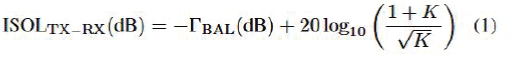 |
| whereK is the tapping ratio of the windings. Equation (1) shows that an RF–dc converter with high efficiency and near
ideal matching is needed, e.g., when K = 1, to get ISOLTX−RX of 50 dB, ΓBAL has to exceed −44 dB. |
| Other applications that require well-controlled rectifier input impedance include rectifying antennas (rectennas),
resonant dc–dc converters, and power recycling in outphasingpower amplifiers. For the rectenna case, the impedance
mismatch between the antenna and the rectifier causes a portion of the available power to be reflected, reducing
conversion efficiency. In a resonant dc–dc converter, the inverter operation and efficiency are highly dependent on the
load resistance offered by the rectifier. In energy recycling outphasing power amplifiers, the rectifier replaces the
isolation resistor in the power combiner. In this case, the rectifier should offer fixed impedance for isolation between,
and proper operation of, the individual power amplifiers, as well as achieving maximum recycling efficiency. |
| In CMOS RF-DC power converter a rectifier for RF identification applications made use of a voltage multiplier with a
reconfigurable number of stages to increase the dynamic range. Tighter control on the input impedance and higher
power tolerance are required for power-recycling applications. |
CLASS-ERECTIFIER ANALYSIS |
| A. Class-E Rectifier |
| A class-E rectifier is the dual of a class-E power amplifier. It was first introduced in 1988 as a new rectifier topology
capable of high-frequency high-efficiency RF–dc conversion. This original topology suffers from variable input
impedance as a function of input power. Class-E power amplifiers achieve significantly higher efficiency than
conventional Class-B or –C amplifiers. In Class-E,the transistor operates as an on/off switch and the load network
shapesthe voltage and current waveformsto prevent simultaneoushigh voltage and high current in the transistor; that
minimizes power dissipation, especially during the switching transitions. Class-E amplifiers can be designed for
narrow-band operation or for fixed-tuned operation over frequency bands as wide as 1.8:1, such as 225-400 MHz. |
| B. RF-DC Converter |
| A DC-to-DC converter is an electronic circuit which converts a source of direct current (DC) from one voltage level to
another. It is a class of power converter. DC to DC converters are important in portable electronic devices such
as cellular phones and laptop computers, which are supplied with power from batteries primarily. Such electronic
devices often contain several sub-circuits, each with its own voltage level requirement different from that supplied by the battery or an external supply (sometimes higher or lower than the supply voltage). Additionally, the battery voltage
declines as its stored power is drained. Switched DC to DC converters offer a method to increase voltage from a
partially lowered battery voltage thereby saving space instead of using multiple batteries to accomplish the same thing.
Most DC to DC converters also regulate the output voltage. Some exceptions include high-efficiency LED power
sources, which are a kind of DC to DC converter that regulates the current through the LEDs, and simple charge pumps
which double or triple the output voltage. |
| The demands on the RF/DC modules are quite high, as the RF - Amplifier and the cavity are sensitive to reflected
power. A proper 50W resistive match over a wide range of power levels has to be maintained. The radiation of
harmonics on the device input must be inhibited. Aspects concerning the reliability, size and cooling have to be taken
into account. |
| 1) Cyclotron Wave Converter (CWC): |
| The CWC device is a new kind of RF to DC converter, patented by V.A. Vanke in 2003. The input RF-Power is used to
accelerate electrons on a spiral path by a classic cyclotron structure. The rotational movement is then converted to an
increase in longitudinal velocity by a specifically shaped external magnetic field. A “depressed collector” catches the
electrons and converts their kinetic energy to a large DC voltage at the load resistance. |
| In RF Recovery using CARA and Depressed Collector the CWC device has been implemented and tested for the
recovery of RF Energy in a particle accelerator. In a simulation the authors were able to predict an overall RF to DC
efficiency of 73% in the S-Band at an input power of 1 MW. This could not be confirmed in measurements because the
electron collector broke down as the output voltage reached 125 kV. At these voltages, considerable engineering effort
is needed to prevent losses through corona discharge, breakdown or even danger by the generation of X -Rays. This
shows that the CWC device is not easily scaled to higher power levels, as the high electron energy and the consequent
high output voltage poses a limitation. |
| 2)Rectenna circuits: |
| The idea of using semiconductors to convert RF-Power to DC has been around since 1964 when W. C. Brown invented
the rectenna. He was able with this combination of antenna and diode-rectifier – to transmit a substantial amount of
power wirelessly. The system operated at 2.5 GHz and used an array of 4480 small signal point contact diodes. The DC
output power was 270 W, enough to build a demonstration helicopter which held itself in the air by RF-Power only. A
At present times RF-Rectifiers are in the focus of research again. Three substantial reasons forthis can be named: |
| • Wireless powered technologies as Radio Frequency Identification are getting more and more popular. |
| • Switch mode power converters are constantly miniaturized. The passive components can only be made smaller by choosing a higher operating frequency – which nowadays reaches the RF area. |
| • Significant advantages in semiconductor materials (band structure engineering) revealed a new generation of
schottky power diodes which can be used up to the RF region. |
| Taking advantage of these points, it is possible to build an RF/DC converter, utilizing semiconductors, which can
handle power levels in the 200 W range and does not suffer the drawbacks of ultra high vacuum devices. This provides
the basis for the energy recovery concept. |
| 3) Conceptual RF/DC Module: |
| A general overview of the proposed RF/DC module is shown in Fig.4. The RF signal from the power divider comes in
through a 50W coaxial cable. |
| A “backup” termination resistor is connected to the input through a circulator. It ensures that the modules do not reflect
RF power under any circumstances – back to the cavity. This approach guarantees a failsafe system, which degrades
gracefully in case of component failures. When a rectifier defect occurs (open or short), the overall recovery efficiency
of the RF/DC array will be degraded but the operation of the particle accelerator will not be restricted in any way. |
| The matching network guarantees an optimum power transfer while not exceeding the maximum voltage or current
ratings of the diode. The small bandwidth (¡2%) of the input signal allows the use of standard resonant matching
techniques. Care must be taken with the design and simulation procedure, as the rectifier is a nonlinear device and its
input impedance is likely to change with different input power levels. The last block is the DC low pass filter and the
actual load. For simulation purposes it is modelled as a simple resistance. In the actual system, multiple module outputs
will be combined to reach usable power levels. |
| C. Varactor Diodes |
| In electronics, a varicap diode, varactor diode, variable capacitance diode, variable reactance diode or tuning diode is a
type of diode whose capacitance varies as a function of the voltage applied across its terminals. The varicap was
developed by the Pacific Semiconductor subsidiary of the Ramo Wooldridge Corporation who received a patent for the
device in June 1961. The device name was also trademarked as the "Varicap" by TRW Semiconductors, the successor
to Pacific Semiconductors, in October 1967. This helps explain the different names for the device as it came into use. |
| 1) Operation: |
| Varactors are operated in a reverse-biased state. No current flows, but since the thickness of the depletion zone varies
with the applied bias voltage, the capacitance of the diode can be made to vary. Generally, the depletion region
thickness is proportional to the square root of the applied voltage; capacitance is inversely proportional to the depletion
region thickness. Thus, the capacitance is inversely proportional to the square root of applied voltage.All diodes exhibit
this phenomenon to some degree, but varactor diodes are manufactured specifically to exploit this effect and increase
the capacitance (and thus the range of variability), whereas most ordinary diode fabrication strives to minimize the
capacitance. |
| The figure shows an example of a cross section of a varactor with the depletion layer formed of a PN junction. This
depletion layer can also be made of a MOS or a Schottky diode. This is very important in CMOS and
MMIC technology. |
| 2) Application: |
| Varactors are used as voltage-controlled capacitors. They are commonly used in voltage controlled
oscillators, parametric amplifiers, and frequency multipliers. Voltage-controlled oscillators have many applications
such as frequency modulation for FM transmitters and phase locked loops. Phase-locked loops are used for
the frequency synthesizers that tune many radios, television sets, and cellular telephones. |
| D. Schottky Diode |
| The Schottky diode (named after German physicist Walter H. Schottky) also known as hot carrier diode is
a semiconductor diode with a low forward voltage drop and a very fast switching action. The cat's-whisker
detectors used in the early days of wireless and metal rectifiers used in early power applications can be considered
primitive Schottky diodes.When current flows through a diode there is a small voltage drop across the diode terminals.
A normal silicon diode has a voltage drop between 0.6–1.7 volts, while a Schottky diode voltage drop is between
approximately 0.15–0.45 volts. This lower voltage drop can provide higher switching speed and better system
efficiency. |
| A metal–semiconductor junction is formed between a metal and a semiconductor, creating a Schottky barrier (instead
of a semiconductor–semiconductor junction as in conventional diodes). Typical metals used are molybdenum,
platinum, chromium or tungsten, and certain silicides, e.g. palladium silicide and platinum silicide; and the
semiconductor would typically be n-type silicon. The metal side acts as the anode and n-type semiconductor acts as the
cathode of the diode. This Schottky barrier results in both very fast switching and low forward voltage drop. |
| Schottky diodes are often used as anti saturation clamps on transistors (a Schottky transistor). Palladium silicide ones
are excellent here due to their lower forward voltage (which has to be lower than the forward voltage of the basecollector
junction); platinum silicide ones have forward voltage closer to that and require more attention in layout. The |
| Schottky temperature coefficient is lower than the coefficient of the B–C junction, which limits the use of PtSi at higher
temperatures. For power schottky diodes the parasitic resistances of the buried N+ layer and the epitaxial n-type layer
become important. The resistance of the epitaxial layer is more important here than for a transistor as the current has to
cross its entire thickness. It however serves as a distributed ballasting resistor over the entire area of the junction and
prevents localized thermal runaway under usual conditions. |
| In comparison with the power p–n diodes the Schottky diodes are less rugged. The junction lies in direct contact to the
thermally sensitive metallization, a Schottky diode can therefore dissipate less power than an equivalent-size p–n one
with deep-buried junction, before failing - especially during reverse breakdown. The relative advantage of lower
forward voltage of Schottky diodes is diminished at higher forward currents, where the voltage drop is dominated by
the series resistance. |
| E. Class-E Rectifier Analysis |
| A class-E rectifier is the dual of a class-E power amplifier. It was first introduced by W. Nitz, W. Bowman, F. Dickens,
F. Magalhaes, W. Strauss, W. Suiter, and N. Zeisse in the paper“A new family of resonant rectifier circuits for high
frequency DC–DC converter applications in 1988 as a new rectifier topology capable of high-frequency high-efficiency
RF–dc conversion. This original topology suffers from variable input impedance as a function of input power. An
analytical model for this dependence is first derived, and then a technique to compensate for it is proposed. |
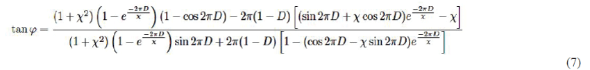
| To simplify the analysis of the class-E rectifier, which is shown in Fig.8 (a), the following approximations can be
made. |
| • The diode dc I–V characteristics can be approximated as piecewise linear, with turn-on voltage VD, forward |
| • resistanceRD, and infinite reverse resistance. |
| • Diode capacitance is assumed linear and is included in C. |
| • All inductances from packaging and wiring are negligible. |
| • The choke impedance at the fundamental and harmonics is much higher than the impedance of C. |
| • The series resonance section formed by Lrand Croffers low impedance at the fundamental frequency only. |
| Fig. 9 shows the simplified circuit model for the rectifier and its two modes of operation: diode on and diode off. In the
diode OFF state (0 ≤ ωt≤ 2π(1 − D)), we can write |
 |
| Solving (2) using the initial condition vD(ωt= 0) = −VD, we obtain |
 |
 |
 |
 |
 |
 |
| The average voltage across the diode <vD>should be equal to the battery voltage VBAT since there is no dc drop across
the RF choke, i.e., |
 |
| Using (2), (3), (5), and (6) in (8), we can relate the diode conduction duty cycle D to other circuit parameters in which,
when solved with (7), completely defines the vDwaveform. |
 |
| The rectifier input impedance can be defined at the fundamental frequency and is related to the vDfundamental
component by |
 |
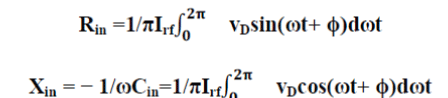 |
| These equations can be solved numerically to find the input impedance. Setting RDand VDto zero results in identical
closed-form relations, which assumed an ideal diode. |
CONSTANT IMPEDANCE OPERATION |
| A.Constant Impedance Operation |
| Impedance is the opposition by a system to the flow of energy from a source. For constant signals, this impedance can
also be constant. For varying signals, it usually changes with frequency. The energy involved can be electrical,
mechanical, magnetic or thermal. The concept of electrical impedance is perhaps the most commonly known. Electrical
impedance, like electrical resistance, is measured in ohms. In general, impedance has a complex value; this means that
loads generally have a resistance component (symbol: R) which forms the real part of Z and areactance component
(symbol: X) which forms the imaginary part of Z. |
| In simple cases (such as low-frequency or direct-current power transmission) the reactance may be negligible or zero;
the impedance can be considered a pure resistance, expressed as a real number. In the following summary we will
consider the general case when resistance and reactance are both significant, and the special case in which the reactance
is negligible. |
| Fig.10 compares the simulated values for the input impedance with the relations derived. It showsthe variation of the
input impedance with RF power at 800 MHz for different values of capacitor Cv. For the simulation, the SPICE model
of a packaged Schottky diode SMS3923- 011LF from Skyworks was used, and a capacitor with fixed part Cfand
variable part Cvwas added in parallel with the diode. Our proposed model shows excellent agreement in the real and
imaginary parts of the input impedance with simulation over the entire input power range of 18 dB. |
| To control the input impedance, capacitor Cvcan be replaced with a varactor diode, whose bias voltage can be
controlled to maintain constant input resistance, whereas the reactive part of the input impedance can be nulled by a
second varactor diode replacing Cr. This combination allows the input impedance to remain constant despite input
power and battery voltage variations.Using varactor diodes to control the rectifier input impedance has another benefit.
Normally, the rectifier is matched to the source only at certain input power level, away from that level a portion of the
power is reflected, degrading efficiency. |
| `The overall power conversion efficiency ηcnvasthe ratio of dc power delivered to the battery power Pdc to available input
RF power Pav, i.e., |
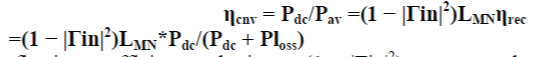 |
| whereΓin is the reflection coefficient at the input, (1 − |Γin|2) represents the power loss due to impedance mismatch,
LMN is matching network loss, and ηrec represents the rectifier intrinsic efficiency.
The output dc power and the total power loss in the rectifier can be given by |
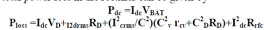 |
| wherercv is the effective series resistance of Cv, and Rrfc is the choke (RFC) dc resistance. The first two terms in the
above equation represent the dominant part of the power loss, which is caused by the diode conduction. Once turned
on, the diode turn-on voltage VDrepresents a constant loss in efficiency. This can be only improved by using lower
barrier diodes, such as Schottky diodes or higher battery voltage, which also increases the peak reverse voltage across
the diode when off. Losses due to RD scale with the input power and require using bigger devices for higher input
power. This also increases the diode junction capacitance and can limit the high-frequency operation. |
| Energy conversion efficiency (η) is the ratio between the useful output of an energy conversion machineand the input,
in energy terms. The useful output may be electric power, mechanical work, or heat.
In an impedance matched network between the RF source and the rectifier, PCE expressed as |
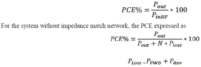 |
| wherePinRFis the average input RF power, Pout is the power delivered to the load, Plossis the total lost power, PFWD
is the lost power due to the channel resistance, and PRevis the power loss due to the sub-threshold leakage current; N is
the number of stages. |
| C. Return Losses |
| S-parameters describe the input-output relationship between ports (or terminals) in an electrical system. For instance, if
we have 2 ports (intelligently called Port 1 and Port 2), then S12 represents the power transferred from Port 2 to Port 1.
S21 represents the power transferred from Port 1 to Port 2. In general, SNM represents the power transferred from Port M
to Port N in a multi-port network. |
| A port can be loosely defined as any place where we can deliver voltage and current. So, if we have a communication
system with two radios (radio 1 and radio 2), then the radio terminals (which deliver power to the two antennas) would
be the two ports. S11 then would be the reflected power radio 1 is trying to deliver to antenna 1. S22 would be the
reflected power radio 2 is attempting to deliver to antenna 2. And S12 is the power from radio 2 that is delivered through
antenna 1 to radio 1. Note that in general S-parameters are a function of frequency (i.e. vary with frequency). |
| By definition, "Return Loss" refers to that portion of a signal that cannot be absorbed by the end of line termination, or
cannot cross an impedance change at some point in the transmission system. This component of the signal is reflected
from the impedance discontinuity and travels back up the line from that point, since it cannot be absorbed by the
termination, or traverse the impedance irregularity. That causes two signals to appear on the coaxial cable, one going in
one direction and the other in the reverse direction. These two signals cancel and add along the line at various points.C |
| When these cancellations occur at a receiving terminal end of the cable, data may be lost forever. This is what causes
concern with regard to return loss on data transmission systems, especially digital video transmission systems. |
| The formula for calculating the amount of Return Loss created by any discontinuity in a coaxial cable is as follows:
Return loss= 20 log10 [(Zt-Zo)/(Zt+ZO)] |
| whereZt = Terminating Impedance |
 |
| Return loss is a matter of serious concern on any transmission system for a digital television signal, and knowing the
magnitude of the return loss at the sending end termination, receiving end termination, and each and every connecting
cable is of primary concern. that is why it is important to measure the return loss of all terminations in your digital
video transmission systems. |
| The most general term for ratioed reflection is the complex reflection coefficient, Γ (gamma). The magnitude portion of
Γ is called ρ (rho). The reflection coefficient is the ratio of the reflected signal voltage level to the incident signal
voltage level. For example, a transmission line terminated in its characteristic impedance Z0, will have all energy
transferred to the load so Vrefl = 0 and ρ = 0. When the impedance of the load, ZL is not equal to the characteristic
impedance, energy is reflected and ρ is greater than zero. When the load impedance is equal to a short or open circuit,
all energy is reflected and ρ = 1. As a result, the range of possible values for ρ is 0 to 1. |
| Reflection Coefficient Γ = Vreflected/ Vincident |
| =|(ZL-ZO)/(ZL+ZO)| |
| Return loss is a way to express the reflection coefficient in logarithmic terms (dB). Return loss is the number of
decibels that the reflected signal is below the incident signal. Return loss is always expressed as a positive number and
varies between infinity for a load at the characteristic impedance and 0 dB for an open or short circuit. Another
common term used to express reflection is voltage standing wave ratio (VSWR), which is defined as the maximum
value of the RF envelope over the minimum value of the RF envelope. It is related to ρ as (1 + ρ)/(1 – ρ). VSWR
ranges from 1 (no reflection) to infinity (full reflection). |
| D.Efficiency and Return Losses v/s input RF Power |
| Fig.12 plots the overall conversion efficiency; it shows that the mismatch severely affects the conversion efficiency
away from the matching condition. With the varactor diode tuning method suggested, matching can be achieved over a
broad range of input power, maximizing the overall efficiency. |
| Control voltage generation for the varactor diodes will depend on the application. In some cases, the control voltages
can be changed to maximize the dc output power. In the hybrid transformer duplexer case, the transmitter leakage at the
receiver side can be sensed, and the varactor diode control voltages can be corrected in a closed-loop manner to
minimize the leakage, or a priori knowledge of the transmitter power can be used to set the optimum values for the
control voltages. |
| Due to the series resonance nature of the input impedance, this converter tends to be narrowband. The bandwidth is
governed by the quality factor of the input series resonant network, and wider bandwidth can be achieved by using
smaller series inductor Lr. The maximum achievable bandwidth will be limited by the capactive part of the rectifier
input impedance. The proposed diode varactors can be used to tune the input impedance with frequency at the cost of
reduced power range. For more demanding applications such as a wideband hybrid transformer duplexer, two or more
rectifiers can be combined in a staggered form to achieve wider bandwidth, as shown in Fig.13. |
| A. Test-board Schematic |
| Fig.14 shows the test board schematic. |
| A two-layer FR4 PCB was designed for operation at 800 MHz with discrete components. A Schottky diode SMS3923-
011LF from Skyworks was used to minimize the diode loss. The diode has a breakdown voltage of 20 V, which is sufficient to withstand a maximum RF power of 27 dBm at a maximum battery voltage of 4.2 V. In addition, two
hyper-abrupt varactor diodes SMV1800-079LF and SMV2019-079LF from Skyworks were used to maximize the
tuning range. |
| B. Measurement Results |
| Fig.15 compares calculated values to simulation and measurements, with the varactor diodes biased for best matching
at input power of 20 dBm. |
| It should be mentioned that, for all calculations, the varactor diodes were replaced with a linear capacitor whose value
is equal to the effective varactor capacitance, and parasitic capacitance values were also estimated from an Agilent
Momentum electromagnetic board simulation. Good agreement is shown for low power; the discrepancy at higher
power is due to high peak forward currents that exceed the range of validity of the SPICE model. Specifically, the
series ohmic resistance of the bulk semiconductor regions of a real diode increases for high-level injection, and it has a
positive temperature coefficient. This leads to increased RDat high power. This mechanism is not accounted for in the
analysis nor in the SPICE model used for simulation. |
| C.Varactor Diode Tuning |
| For measurements, the input frequency was fixed at 800 MHz and input power was swept from 10 to 27 dBm. Fig.16
shows the large signal S11 and power conversion efficiency ηcnv = Pdc/Pavas a function of the available source power. |
| The figure show the case with a fixed varactor bias (a traditional class- E rectifier); then, the case where the two
varactor biases are changed to minimize S11. Both simulated and measured data are shown. With varactor tuning, S11 is
less than −20 dB for approximately 12 dB of RF power variation. This was verified across the whole range of a lithiumion
battery voltage from 2.5 to 4.2 V, which is a significant improvement compared with the no-tuning case. The
improved S11 improves conversion efficiency as less power is reflected, particularly for lower power levels where
matching loss dominates. At higher power levels, the diode loss dominates due to the diode series resistance, and better
matching results in more power going to the diode, which amplifies its series resistance increase, further limiting the
improvement to about 2%. Efficiency improves with higher battery voltage, which also increases the peak reverse
voltage across the diode. The peak measured efficiency of 60% occurs at VBAT = 4.2 V and Prf = 17 dBm. |
CONCLUSION |
| An RF–dc converter with well-controlled input impedance and high efficiency over a wide range of input power has
been shown. The operation of the class-E rectifier was analyzed, and a new technique for controlling its input
impedance has been presented. The technique depends on two varactors to compensate for input power and dc load
variation. A PCB was designed at 800 MHz with commercial components, achieving a peak efficiency of 60% with S11
less than −20 dB over 12-dB input power variation and 2.5–4.2 V battery voltage change. This concept can be applied
to energy recycling applications where the rectifier closely emulates a load resistor without the power loss included in a
real load. The technique achieves a wider dynamic range with good efficiency. |
Tables at a glance |
 |
| Table 1 |
|
| |
Figures at a glance |
 |
 |
 |
 |
| Figure 1 |
Figure 2 |
Figure 3 |
Figure 4 |
 |
 |
 |
 |
| Figure 5 |
Figure 6 |
Figure 7 |
Figure 8 |
 |
 |
 |
 |
| Figure 9 |
Figure 10 |
Figure 11 |
Figure 12 |
 |
 |
 |
 |
| Figure 13 |
Figure 14 |
Figure 15 |
Figure 16 |
|
| |
References |
- An RFâÃâ¬ÃâDC Converter with Wide-Dynamic-Range Input Matching for Power Recovery ApplicationsâÃâ¬ÃÂ; SherifH.Abdelhalem, Prasad S. Gudem, Member, IEEE, and Lawrence E. Larson, Fellow, IEEE; Vol. 60, No. 6, June 2013
- M. Mikhemar, H. Darabi, and A. Abidi, âÃâ¬ÃÅA tunable integrated duplexer with 50 dB isolation in 40 nm CMOS,âÃâ¬Ã in Proc. ISSCC Dig. Tech. Papers, Feb. 2009, pp. 386âÃâ¬Ãâ387.
- S. Abdelhalem, P. Gudam, and L. Larson, âÃâ¬ÃÅA tunable differential duplexer in 90 nm CMOS,âÃâ¬Ã in Proc. RFIC Symp., Jun. 2012, pp. 101âÃâ¬Ãâ104.
- H. Takhedmit, B. Merabet, L. Cirio, B. Allard, F. Costa, C. Vollaire, and O. Picon, âÃâ¬ÃÅA 2.45-GHz dual-diode RF-to-DC rectifier for rectennaapplications,âÃâ¬Ã in Proc. EuMC, Sep. 2010, pp. 37âÃâ¬Ãâ40.
- Y. Han, O. Leitermann, D. A. Jackson, J. M. Rivas, and D. J. Perreault, âÃâ¬ÃÅResistance compression networks for radio-frequency power conversion,âÃâ¬Ã IEEE Trans. Power Electron., vol. 22, no. 1, pp. 41âÃâ¬Ãâ53, Jan. 2007.
- R. Langridge, T. Thornton, P. M. Asbeck, and L. E. Larson, âÃâ¬ÃÅA power re-use technique for improved efficiency of outphasing microwave poweramplifiers,âÃâ¬Ã IEEE Trans. Microw. Theory Tech., vol. 47, no. 8, pp. 1467âÃâ¬Ãâ 1470, Aug. 1999.
- P. A. Godoy, D. J. Perreault, and J. L. Dawson, âÃâ¬ÃÅOutphasing energy recovery amplifier with resistance compression for improved efficiency,âÃâ¬Ã IEEE Trans. Microw. Theory Tech., vol. 57, no. 12, pp. 2895âÃâ¬Ãâ2906,Dec. 2009.
- S. Scorcioni, A. Bertacchini, and L. Larcher, âÃâ¬ÃÅA 868 MHz CMOS RFâÃâ¬ÃâDC power converter with -17 dBm input power sensitivity and efficiencyhigher than 40% over 14 dB input power range,âÃâ¬Ã in Proc. ESSCIRC, Sep. 2012, pp. 109âÃâ¬Ãâ112.
- W. Nitz,W. Bowman, F. Dickens, F. Magalhaes,W. Strauss,W. Suiter, and N. Zeisse, âÃâ¬ÃÅA new family of resonant rectifier circuits for high frequencyDCâÃâ¬ÃâDC converter applications,âÃâ¬Ã in Proc. Appl., Power Electron. Conf.,Feb. 1988, pp. 12âÃâ¬Ãâ22.
- M. K. Kazimierczuk, âÃâ¬ÃÅAnalysis of Class-E zero-voltage-switching rectifier,âÃâ¬Ã IEEE Trans. Circuits Syst., vol. 37, no. 6, pp. 747âÃâ¬Ãâ755, Jun. 1990.
- A. Noda and H. Shinoda, âÃâ¬ÃÅCompact class-F RFâÃâ¬ÃâDC converter with antisymmetric dual-diode configuration,âÃâ¬Ã in Proc. IEEE MTT-S Int. MTT, Jun. 2012, pp. 1âÃâ¬Ãâ3.
- âÃâ¬ÃÅElectronic Devices and CircuitsâÃâ¬ÃÂ; J.B.Gupta; Katson Educational Series, 3rd edition.
- âÃâ¬ÃÅDesign concepts for RF-DC conversion in particle accelerator systemsâÃâ¬ÃÂ; F. Caspers, M. Betz, A. Grudiev CERN, Geneva, Switzerland; H. Sapotta, Karlsruhe University of Applied Sciences, Germany
- âÃâ¬ÃÅReturn LossâÃâ¬ÃÂ; Frank McClatchie; F M Systems,Inc.
- Electronic Devices and Circuit TheoryâÃâ¬ÃÂ; R E Boylstead and L Nashelsky:, 9/e, Pearson Education.
- Wikipedia:Class-E power amplifiers, S11 parameters, Input impedance, Output impedance, Impedance matching, Return losses.
|