Keywords
|
| Single phase rectifiers, mathematical model, bidirectional AC-DC converters. |
INTRODUCTION
|
| The single-phase voltage source PWM rectifier (VSR) is widely used in improving the quality of the power energy. Recently, lots of researches have been investigated for the Single-Phase PWM rectifier. The single-phase PWM rectifier is now becoming more and more popular due to its low distortion input current, unity power factor operation and bi-directional power flow ability. As the filter capacitor required is generally small under balanced supply voltage conditions, it may also be believed that these converters can offer excellent dynamic response of the dc output voltage. In general, the selection of an appropriate controller of a PWM rectifier in consideration of stability and dynamic performances requires good knowledge about the characteristics of the system to be controlled. Various strategies have been applied on the single-phase PWM rectifier, such as states-space averaging and circuit methods. |
| A three-phase PWM rectifier is often used together with closed-loop dc–dc converters as loads. The three phase PWM rectifier can be compared with the working of DC-DC boost converter. SISO model can be derived for the three phase PWM rectifier so that it can be comparable with the DC-DC boost converter. In this paper, the suitable controller for small signal transfer function model for single phase PWM rectifier was designed under closed loop operation and also SISO model, controller for closed loop operation of three phase rectifier was designed. |
BOOST RECTIFIER
|
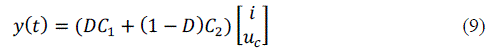
| Single-phase PWM rectifier based on the small signal model are dealt in detail. The purpose is to decrease the voltage fluctuations and increase the dynamic performance of the rectifier when the load changes suddenly. The procedure for deriving the transfer function are to make assumptions then define the state variables and write state equations for each interval of operation, average the state equations over a switching cycle and introduce perturbation in state variables then equate ac and dc quantities and proceed with ac equations and take Laplace transform, prepare matrix Small signal model and calculate desired transfer functions |
| The fig.1. shows the basic equivalent circuit of single phase PWM rectifier. Fig.2. and Fig.3 shows the mode of operation for PWM rectifier acting as a boost rectifier. PWM rectifier can be used as bidirectional rectifiers. Rectifier operation is performed by the diodes, while the inverter operation is performed by switches. As tabulated in table 1, it can operate the rectifier in a boost mode by controlling the switches T1,T2 with the help of the inductor at source. |
| Under steady state operation, mode 1, when switch T2 is ON, the conduction path is given by VS-L-T2-D4. Hence the inductor is charging, since there is no connection to the load. This mode of operation is similar to that of the DC-DC boost converter operation when switch is ON. In Mode 2, when T2 is OFF, the conduction path will be VS-LD1- load-D4. Here the inductor is discharing mode. More over the switches T3 and T4 has no effect on the operation of a boost rectifier. |
DESIGN OF CONVERTER PARAMETERS
|
| Inductor and capacitor will play a major role in the boost rectifier as shown in the operation. Inductance is used for bi-directional power flow and boost operation, while the capacitance is used to maintain the constant DC output for a period of time by reduce the output DC ripples. Hence designing of inductance and capacitance have a significant role in the operation. Moreover the modulating index must be less than 1 for PWM pulse. Hence the amplitude of modulating signal must be greater than of the amplitude of carrier signal.A. VOLTAGE GAIN: |
| A. VOLTAGE GAIN: |
| The boost voltage obtained in the output can be calculated by |
| Vo=Vs*M.I/(1-d) (1) |
| Where, M.I = Modulating index |
| d = switching period |
| B. INDUCTANCE: |
| The fundamental component of PWM switch should be given by Vr. It should be varied from the supply voltage at an angle of δ as the line is similar to that of transmission line. |
| The inductance can be derived as follows |
| Vr=Fundamental component of PWM waveform |
| Vs= Supply Voltage, Is= Supply currents |
 |
| From the above equation we can find L as |
 |
| C.CAPACITANCE: |
| IL, the load current contains DC current and ripple current. Capacitor makes IL perfect DC and ripple should be maximum of 5%. By equating output power equals to input power and equate IL with the AC part we can obtain the value of capacitance as follows |
 |
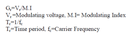
| D.CARRIER FREQUENCY: |
| The carrier frequency should be minimum in the order of 11*fs, where fs is the supply or fundamental frequency. For 50Hz supply it should be above 550Hz. Most probably 2KHz is chosen. |
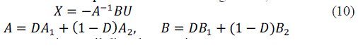
SMALL SIGNAL MODEL
|
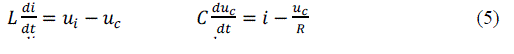
| Assume all of the switches are ideal time-variant switch model. Also, suppose the inductor current and the capacitor voltage is state variable. Then we can get the math model when the switches turn on/off. The mathematical model can be calculated as |
 |
 |
| So the following equations show the ideal small signal model |
 |
| A. AVERAGE STATE EQUATION: |
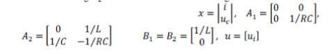
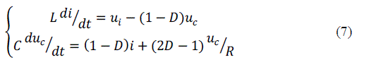
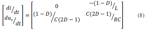
| The first step is to use the average state function instead of the two partition state functions. According to the proportion weighted average of the state function in on/off state, we get the state space average model in on switchperiod. Assume D is the average of the switch variable |
 |
 |
 |
| B. PERTURB AND LINEARIZATIONWe know that low frequency and small ripple characteristic of the rectifier is satisfied, so the derivative of state vector in stable state equals to zero. According to that, we obtain that |
 |
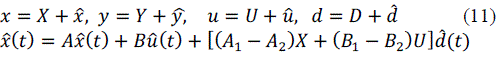 |
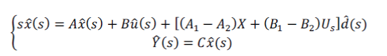 |
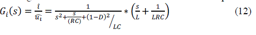
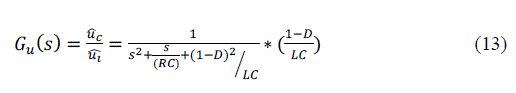
| C. TRANSFER FUNCTION: |
| So we get the transfer function of state variable and output variable expressed as |
 |
 |
CLOSED LOOP CONTROL:
|
| The closed loop control consists of inner current loop and outer voltage loop. The inner loop needs a current controller and outer loop requires a voltage controller. The overall block diagram of closed loop control for single phase rectifier is given as follows |
| The comparison of Vref and V0 produce changes in capacitor voltage, change in capacitor voltage which in turn alter the output current, as output power is equal to input power change in output current will alter the input current. Hence the controller output is given as Is*(referrence supply current). To match Is* and Is it produce fundamental component of Vr. If I0 matches Iload , no fluctuations in capacitor voltage, but in case not matches means it will produce fluctuations in capacitor voltage and as mentioned above all the parameters alter in order to match the fluctuations. If we add a product block, multiplying with a sign term which is in phase with Vs, then it will give Vs and Is in phase with each other, which means UPF in input side. |
| A. INNER CURRENT LOOP CONTROL: |
| B. CONVERTER: |
 |
| `C. OUTER VOLTAGE LOOP: |
| D. CONTROLLER DESIGN: |
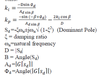
| Input current regulation in the converter is achieved by adjusting the duty cycle. Generally three basic algorithm used are P, PI and PID. Here PI controller in the Inner current loop which regulate the input current, reduce peak over shoot and steady-state error.The PI consists of two basic modes that are proportional modes and integral modes. A proportional controller (kp) reduced settling time and reduced the error but not eliminated it. An integral controller (ki) will have the effect of eliminating the steady-state error. Limiter is used to control the duty cycle within the desirable band. |
 |
| The physical model of closed loop control is given as follows |
| E. SIMULATION RESULTS: |
| Fig.8. shows the inner current loop control and fig.9 shows the outer voltage loop control of a single phase PWM rectifier. Fig.10. shows the combination of inner current loop and outer voltage loop. Fig.11. shows the inner current loop settling for change in reference current. Fig.12. shows the outer current loop settling for different output voltages. Fig.13. the simulated waveform shows the inner current loop settles for different source voltage(Vs). Fig.14. shows the outer voltage loop settles for different load currents. The closed loop control using physical model is simulated with the Vref is given as 400V. The simulation output representing the output voltage settles at 400V is given in the fig.15. and the input current is stabilized using inner current loop which makes input current and voltage in phase,(UPF) is given in the fig.16. |
| Here the PI controller is designed as Kp=.99724,Ki=53.3. Iref=4A, here after the initial oscillations and peak over shoot, it settles with the given reference value. For outer voltage loop the PI controller is designed as Kp=.913,Ki=2.27,The Vref=400V. |
SISO MODEL FOR THREE PHASE PWM RECTIFIER
|
| A. INTRODUCTION: |
| A SISO model is constructed by splitting the d-axis and q-axis by nonlinear feed forward decoupling and maintaining nearly unity power factor operation. This system is possible to extend the analysis and control design techniques of dc– dc converters to the three-phase PWM rectifier also. The usefulness of the model is demonstrated through closed-loop operation of the rectifier with both voltage mode and inner-current-loop-based schemes. |
| B. THREE PHASE PWM RECTIFIER: |
| Over the past several years, considerable research work has been carried out on the control of ac-to-dc Pulse width modulation (PWM) rectifiers, since these converters possess many desirable features such as sinusoidal line currents at a required power factor, a nearly constant dc output voltage, and bidirectional power delivery capability. As the filter capacitor required is generally small under balanced supply voltage conditions, it may also be believed that these converters can offer excellent dynamic response of the dc output voltage. |
| Control of three-phase PWM rectifiers in the d–q synchronously rotating frame (SRF) has been developed from field oriented control techniques for ac drives in early 1980s. Normally, the control objectives of a PWM rectifier are to regulate the dc output voltage on the dc side, achieve unity power factor (UPF) operation on the ac side, and also to achieve fast dynamic response to line and load disturbances. A state-space averaged model has been proposed for the three-phase PWM rectifier in the d–q SRF. However, the model, though accurate, does not give sufficient insight into the controller design and behaviour of the three-phase PWM rectifier system due to its complex multi input–multi output (MIMO) nonlinear structure and the presence of a non minimum phase feature. Due to this, designing a proper controller for such a converter has been generally a challenging task. The SISO model equation has been derived in [1]. It deals with the closed loop control of three phase rectifier with siso model. |
| C. EQUIVALENT CIRCUIT FOR SISO MODEL: |
| D. NON LINEAR FEEDFORWARD DECOUPLING CONTROLLER: |
| In Fig.19. the coupling terms between the d-axis and the q-axis are represented by the two current-controlled dependent voltage sources. Decoupling may be achieved, if the effects of these two voltage sources are nullified by appropriately adjusting the control inputs vd and vq |
| E. CLOSED LOOP CONTROL: |
| It is well known that the output performance of a single-phase power factor correction unit is limited by the slow response of the bulky capacitor. This drawback is overcome by a three-phase PWM rectifier as it successfully gets rid of the line-frequency related ripple on the dc side. This allows ripple-free output voltage operation to be achieved even with a small filter capacitor. Here, Fi(s) is the control to- d-axis current transfer function given in [1]. In designing a multiloop controller, one first designs the inner loop. Here the controller used is PI controller. Once the current loop is closed, the converter can be treated as a new open-loop plant with transfer function Fvi(s) given in [1].Here this acts as a outer voltage loop model. |
| F. SIMULATION RESULTS: |
| Fig.21. shows the inner current loop design with a PI controller and Fig.22. shows the outer voltage loop control. |
| Here the closed loop is designed for input voltage Ed=230V, L can be designed as .003H and C=.000136F. The controller used is PI controller and Kp propotional constant is kept unity, while Ki integral constant is designed as 53.3 in Time domain to reduce the steady state error |
CONCLUSION
|
| The physical model and mathematical model are designed for single phase rectifier. The closed loop control for single phase PWM rectifier with PI controllers also designed using mathematical model and verified with physical model. SISO model for three phase rectifier and closed loop control are designed for a three phase rectifier. Simulation is done using MATLAB and the simulation results are shown. In future the mathematical SISO model can be simulated. |
Tables at a glance
|
 |
| Table 1 |
|
| |
Figures at a glance
|
 |
 |
 |
 |
 |
| Figure 1 |
Figure 2 |
Figure 3 |
Figure 4 |
Figure 5 |
 |
 |
 |
 |
 |
| Figure 6 |
Figure 7 |
Figure 7a |
Figure 8 |
Figure 9 |
 |
 |
 |
 |
 |
| Figure 10 |
Figure 11 |
Figure 12 |
Figure 13 |
Figure 14 |
 |
 |
 |
 |
 |
| Figure 15 |
Figure 16 |
Figure 17 |
Figure 18 |
Figure 19 |
 |
 |
 |
| Figure 20 |
Figure 21 |
Figure 22 |
|
| |
References
|
- Bo Yin, Ramesh Oruganti, (2009) “A Simple Single-Input–Single-Output (SISO) Model for a Three-Phase PWM Rectifier”, IEEE Trans. Ind. Electron.Vol. 24, No. 03, Nov 2009.
- B. Yin, R. Oruganti, S. K. Panda, and A. K. S. Bhat, “Experimental verification of a dual single-input single-output (SISO) model of a threephase boost-type PWM rectifier,” in Proc. 31st IEEE Conf. Ind. Electron. Soc., 2005, pp. 1030–1035.
- S. Hiti, D. Boroyevich, and C. Cuadros, “Small-signal modelling and control of three-phase PWM converters,” in Proc. Ind. Appl. Soc. Annu. Meeting, Oct. 1994, vol. 2, pp. 1143–1150.
- B. Yin, R. Oruganti, S. K. Panda, and A. K. S. Bhat, “Performance comparison of voltage mode control and current mode control of a three-phase PWM rectifier based on dual SISO model,” in Proc. 32nd IEEE Conf. Ind. Electron. Soc., Paris, France, Nov. 2006, pp. 1908–1914.
- Jiang Wei “Analysis And Design Of A Single-Phase PWM Rectifier Based On The Small Signal Model” 978-1-4244-4994-1/09 ©2009
- Robert B.Erickson “Fundamentals of Power electronics”.
|