Keywords
|
| Resonant Converters, ZCS, Current mode & Digital controller |
INTRODUCTION
|
| Resonant converters have gained importance owing to certain advantages of switching sinusoidal voltages and currents. These converters use an L-C resonant circuit for switching the semiconductor devices when they are at the zero current or zero voltage point; this reduces the switching stress on the device and minimized the higher frequency harmonics thereby reducing noise levels. Another advantage of the resonant converters is that the inductors and capacitors, which appear as undesirable parasitic in hard switching topology, are utilized as the resonant inductor and capacitor needed for the resonant switch circuit. There are two types of quasi-resonant switches: the current mode and voltage mode quasi-resonant switches[1-3]. For the current mode, the inductor of the resonant tank circuit is connected in series with the switching transistor to shape the current flowing through it. This paper focuses on the Zero Current switching (ZCS) full bridge buck converter based on the current mode. Simulation studies for the proposed ZCS buck converter is carried out using PSPICE. A digital controller has been proposed and a prototype has been built to validate the results. |
RELATED WORK
|
| In [1], the authors have discussed about the resonant switch topologies operating under the principle of zerocurrent switching (ZCS) and zero-voltage switching (ZVS) to minimize switching losses, stresses, and noises. Using the resonant switch concept, a host of new quasi-resonant converters (QRCs) are derived from conventional PWM converters. They are capable of operating in the megahertz range, with a significant improvement in performance and power density. Performances of ZCS and ZVS QRCs are compared. Power stages, gate drives, and feedback controls are discussed. In [2,3], the authors have discussed three classes of zero- voltage soft-switching PWM converters (namely the zero-voltage switched (ZVS) quasi-square-wave converters, ZVS-PWM converters, and zero-voltage-transition PWM converters) and two classes of zero-current soft-switching PWM converters (namely, the zero-current-switched PWM converters and zerocurrent- transition PWM converters) are reviewed, and their merits and limitations are assessed. Experimental results of several prototype of converters are presented to illustrate each class of converters. |
ZERO CURRENT SWITCHING QUASI-RESONANT BUCK CONVERTER (ZCS-QRC)
|
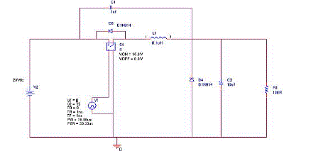
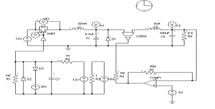
| Fig.1 shows the ZCs quasi-resonant buck converter and its analysis can be simplified considerably by making the following assumptions [4,5]. The output filter and Ro can be treated as a constant-current sink of Io. The switching devices are ideal semiconductor devices with no forward drop in their on-state and no leakage currents in their off-state. There are also no time delays at either turn-on or turn-off. The resonant inductor and resonant capacitor are ideal circuit elements with no loss or parasitic elements. The output inductance Lo is assumed to be much smaller than the resonant inductance Lr. |
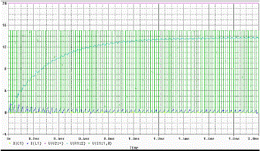
| This converter uses an L-C resonant tank to shape the current and voltage waveforms of the MOSFET switch and hence brings about the zero current condition. At the instant when the current through the switch goes to zero, PWM pulses are generated to fire the MOSFET. The proposed converter is simulated in PSPICE and the simulation parameters are Vin = 20V, C1 = 1uF, L1= 0.1uH, C2= 10uF and R= 100ohms.Figure6.2 represents the various waveforms related to the simulated circuit. It shows a series of PWM firing pulses that produces a stabilized output voltage for a given input voltage. |
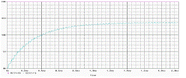
| The given DC input of 20V produces an output voltage of around (14-15) V as shown in Figure6.3. |
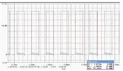
| Fig.4 represents the PWM pulses generated to fire the switch at the instant of zero current through it. |
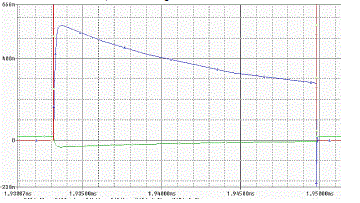
| The condition of zero current through the switch is illustrated in the Fig.5. This figure also depicts that the PWM pulses are generated exactly at the instant of zero current, thus switching on the MOSFET. |
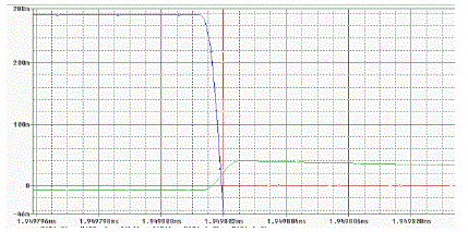
| Just at the instant when current through the switch becomes zero, the MOSFET is turned off, hence achieving zero current condition (Fig.6). |
PWM TECHNIQUES EMPLOYED FOR THE PROPOSED RESONANT CONVERTER
|
| The technique of modulating the on and off pulses that are applied to the switching transistor is called pulse width modulation . Depending on the control signals required to achieve the PWM operation, there are two modes of PWM operation[6-7]: |
| • Analog PWM Operation |
| • Digital PWM Operation |
ANALOG PWM OPERATION
|
| The analog PWM operation can be split into: voltage mode PWM controller and current mode PWM controller. The voltage mode PWM controller derives its control signal from the output voltage of the switching converter as shown in Fig.7. It consists of an error amplifier, open-loop PWM comparator, switching logic and a base drive circuitry that drives the switching transistor through the switching logic. The comparator PWM signal output is used to drive the AND gates in the switching logic, enabling each output only when both inputs to the gate are “high”. The PWM pulses along with the output voltage waveform is shown in Fig.8. |
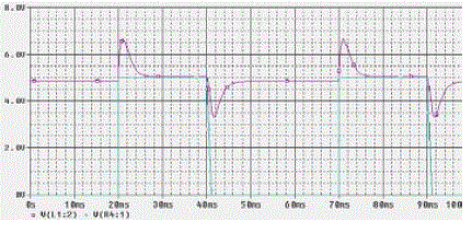
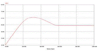
| Current mode PWM controller uses both voltage and current information of the inductor of the switching transistor to get the desired duty cycle. The duty cycle of the switching converter is determined by the times at which the switch current reaches a threshold value. The simulation result shows the stabilized output voltage waveform (refer Fig.10) with respect to the proposed controller for the converter . |
| The advantages of current mode over voltage mode are as follows : |
| • In current mode PWM controller, failure due to excessive current can be prevented by simply limiting the maximum value of the control signal, which is not possible in voltage mode PWM controller. |
| • Switching converters can be operated in parallel without a load-sharing problem. |
| • Current-mode PWM controller simplifies feedback network design. |
| The digital PWM technique employs micro-controller for generating firing pulses for the switching transistors. They also offer a wide range of advantages over the analog PWM technique. |
| • Digital PWM techniques have higher accuracy and higher processing speeds, thus having a faster execution time (in the order of micro-seconds). |
| • They have a higher temperature range of operation. |
| • Digital PWM technique offers better resolution. |
| • Analog PWM technique generally consists of an error amplifier, PWM comparator and a ramp signal generator. |
| • Analog PWM circuits are inexpensive, but they contain discrete components which make the circuit highly complex. |
| Hence, the usage of digital PWM technique for generation of firing pulses proves to be easier and more efficient. PIC micro-controllers are being extensively used for the generation of PWM pulses for switching converters. |
EXPERIMENTAL RESULTS
|
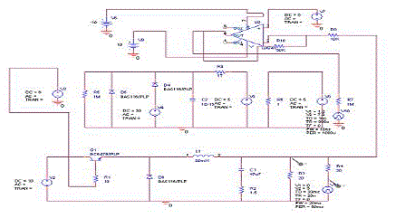
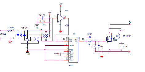
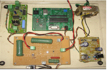
| A prototype of the proposed quasi resonant buck converter is built using IRF840MOSFET, freewheeling diodes D1N914, PIC microcontroller, resonant capacitors of 1uF, 100uF and inductors of 0.1uH .Optocoupler and driver circuit is shown in Fig.11.Fig.12 shows the prototype of the quasi-resonant DC-DC converter . |
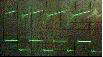
| Fig.13 shows the waveforms representing the PWM pulses and the inductor current depicting the zero current switching condition for the proposed converter. |
CONCLUSION
|
| A full-wave, current-mode ZCS quasi resonant DC-DC Buck converter has been designed and analyzed. The operation of the converter in open loop has been studied. The PWM pulses for firing the switch (MOSFET) are given using PIC Microcontroller. The key feature of this converter is that a nearly lossless switch turn on/off is achieved with a soft turn on/off instead of hard switching. ZCS has been achieved by constructing a prototype Buck converter which shows that the turnoff losses can be reduced. |
Figures at a glance
|
 |
 |
 |
 |
 |
| Figure 1 |
Figure 2 |
Figure 3 |
Figure 4 |
Figure 5 |
 |
 |
 |
 |
 |
| Figure 6 |
Figure 7 |
Figure 8 |
Figure 9 |
Figure 10 |
 |
 |
 |
| Figure 11 |
Figure 12 |
Figure 13 |
|
| |
References
|
- Fred C. Lee (1988), “High-Frequency Quasi-Resonant Converter Technologies”, Proceedings of the IEEE, Vol. 76, No. 4, pp.377-390.
- Hua G. and Lee F.C. (1995), “Soft-Switching Techniques in PWM converters”, IEEE Trans. Indus. Electron., Vol. 42, No. 6, pp.595-603.
- Khai D.T. Ngo (1987), “Generalization of Resonant Switches And Quasi-Resonant DC-DC Converters”, IEEE PESC, 1987 Record, pp. 395-403.
- Libano F. B, J.C.O. Bolacell, D.C. Martins and I. Barbi (1990), “Buck Quasi-resonant Converter Operating at Constant Frequency: Analysis,Design And Experimentation”, IEEE Trans. Power Electron., Vol. 5, No. 3 pp.276-283
- Ned Mohan, Tore M. Undeland and William P. Robbins (1989), “Power Electronics: Applications And Design”, Copyright by John Wiley &Sons.
- Petkov R. (1995), “Quasi-Resonant Power Converter”, NZ Patent Application No. 299312.
- Simon S. Ang (1995), “Power Switching Converters; Electrical Engineering And Electronics Book”, Copyright by Marcel Dekker.
|