Keywords
|
| A symmetrical half-bridge (AHB) converter, half bridge (HB) LLC converter, hold-up time, personal computer (PC)power supplies, server power system. |
INTRODUCTION
|
| The necessity of the power supplies with a high efficiency is emphasized on medium power (300-600W) supplies due to the server infrastructure for small companies and demand for the office computer. As a result, many high efficiency dc/dc topologies have been developed for these medium power applications, which require the hold-up time conditions and high output current. The effort to obtain ever-increasing power density and high voltages over entire load conditions the switching devices have to be made turn ON and turn OFF over wide load range. Due to continuous turn ON and OFF, high di/dt experience high voltage stress thus dv/dt also forms. Due to these the power losses should be increased, more power is dissipated and thus decrease the efficiency, and also increase the size of the component. This can be eliminated by changing the switching frequencies to operate at higher frequencies which will limits the size of passive components, such as transformers and filters; however, switching losses have been obstacle to high- frequency operation, resonant switching techniques have been developed. These techniques process power in a sinusoidal manner and switching devices are softly commutated. |
| The proposed converter half-bridge LLC converter is one of the popular converter in medium power applications because of No transformer DC-offset current, wide range ZVS, low voltage stress. Since it has no output inductor, the snubber losses can be eliminated. The soft switching techniques reduce the size and cost of the converter. |
CIRCUIT TOPOLOGY
|
| The block diagram for the conventional Half-Bridge converter as shown in figure.1. Initially the applied dc voltage to switching bridge generates a square wave form to excite the resonant tank, the resonant sinusoidal current gets rectified or scaled by transformer and rectified output gets filtered by output capacitor to obtain regulated DC voltage. |
| A. Circuit Diagram Of Conventional HB Converter |
| The pulse frequency modulation (PFM) half-bridge converter has been proposed in [1], controls the output voltage across the primary the primary blocking capacitor according to the switching frequency, and it has no freewheeling period with the aid of 50% fixed duty cycle. Therefore, it decreases the transformer turns ratio and conduction losses in primary switches. The circuit diagram of proposed converter shown in figure.2. has half bridge converter with MOSFETS switches Q1 and Q2. The resonant tank with blocking capacitor CB, resonant inductor Llkg and it also known as leakage inductance. This both resonant capacitor and resonant inductor initially resonates at particular frequency and produces sinusoidal currents to regulate the DC off set voltages. Along with this an Magnetizing inductance Lm is also present. This also resonates with another frequency. |
| In order to achieve a high efficiency over entire load conditions for a wide-input-voltage and high-output-current applications such as server power supplies and PC power supplies, a new Half-Bridge (HB) converter, which employs one additional switch QA and capacitor CA, is proposed as shown in figure.1. The primary switches Q1 and Q2 of the proposed converter are complementarily made turn-on and turn-off by PFM with a 50% duty cycle, and additional switch is turned on and turned off according to the input voltage/output load condition. |
OPERATIONAL OF PROPOSED CONVERTER
|
| The circuit diagram shown in figure.1.is the proposed converter, compared with PFM HB converter, one additional switch and capacitor are employed in secondary side made turn on when load is less than 30% of actual one. Here the primary switches Q1 & Q2 are made complementarily ON & OFF by 50% duty cycle also known as pulse frequency modulation (PFM). Each cycle can be divided into two half-cycles t0-t2 and t2-t4 for below above load conditions. |
| A . Above 30% load conditions |
| Initially the proposed converter may acts as PFM HB resonant converter by turning off the additional switch along with capacitor. |
| Mode 1: [t0-t1] |
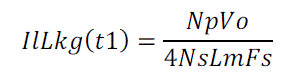
| When Q1 is turned ON at t0 the power is transferred from input to output. In secondary side the rectifier switch SR1 is turned ON at the same time interval. Thus the load current Io is reflected to the primary side of the transformer and an voltage is dropped across magnetizing inductance (Lm). Due to this there will be current flow in the circuit i.e., resonant leakage current (ILlkg) and magnetizing current (ILm). |
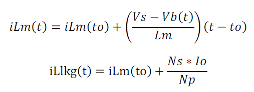 |
| Mode 2: [t1-t2] |
| At time t1 the switch Q1 is made turn OFF and the currents iLlkg and iLm are discharged and now the magnetizing inductance is resonated with the capacitor (Cb). Here the voltage reaches zero linearly. At this time, the anti parallel diode of Q2 conducts. Therefore, the ZVS of Q2 can be achieved. |
| B. Below 30% load conditions: |
| To improve the efficiency over entire load conditions the additional switch made turn on along with capacitor which will reduces voltage stress on the primary switches and conduction losses also. |
| Mode 1: [t0-t1] |
| The switch Q1 is turned ON the energy is transferred from input to output, Since SRI is turned on, iLm(t) is linearly The operational key waveforms for each case are respectively shown in Figure.3. |
ANALYSIS OF PROPOSED CONVERTER
|
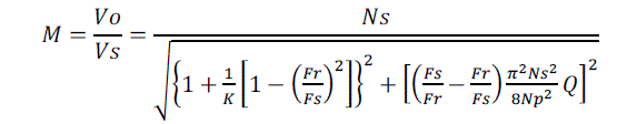
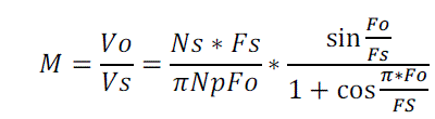
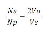
| A. DC conversion ratio: |
| Since the proposed converter operates like the HB LLC converter below 30% load conditions, its DC conversion ratio below 30% load conditions can be represented as follows: |
 |
The two different frequencies at which the converter resonates are given as below: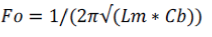 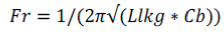 Where Fo= Operating Frequency, Fr= Resonant Frequency Where Fo= Operating Frequency, Fr= Resonant Frequency |
| Furthermore, since the proposed converter operates like the PFM HB converter at above 30% load/hold-up time conditions, its DC conversion ratio at above 30% load/hold-up time conditions can be represented as follows [ 10]: |
| B. Switch turn off losses below 30% load conditions: |
 |
| The switch turn-off loss is mainly determined by the switch current at the turn-off instant. As can be seen in Fig. 3(a) and 3(b), the primary and secondary turn-off switch currents of the proposed converter are less than those of the conventional PFM HB converter due to a sinusoidal-shaped current, which results in much less switch turn-off losses. However, this resonant operation causes a little high conduction losses in the primary and secondary switches at light load conditions, where the conduction loss is not a dominant factor at light load efficiency. Output filter capacitor may be given by |
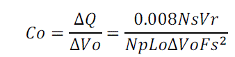 |
| Additional switch capacitor at below 30% load conditions may be given by |
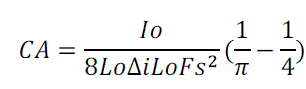 |
| where Io is the output load current and iLo is the output inductor current ripple. The transformer turns ratio can be given by |
 |
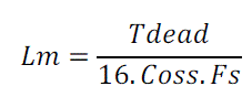
| As explained in Mode 2 below 30% load conditions, the proposed converter operating in resonant region achieves the ZVS turn-on of the primary switches by peak magnetizing inductor current, to ensure the ZVS turn-on, peak magnetizing inductor current should discharge the switch output capacitor within the dead time between the primary switches, which is expressed as follows: |
 |
 |
| MATLAB/SIMULINK is used for the simulation studies. |
| The figure.4. shows the proposed LLC HB resonant converter simulation module at above 30% load condition. |
| The figure.5. shows input DC voltage of proposed converter with (340-400)v which is nominal value and this voltage will be further made as square waveform with 50% duty cycle. |
| The figure.6. shows gate pulses of half-bridge converter with PFM of 50% duty cycle. This will excite the resonant tank and maintain the required current. |
| The figure.7. shows resonant blocking capacitor voltage which was involved in resonance with magnetizing inductor and resonant inductor at two different frequencies. |
| The figure.8. shows current waveforms of resonant inductor Lr and the magnetizing inductor Lm which exhibits zero voltage switching and zero current switching which are known as soft witching. |
| The figure.9. shows output alternating voltage of resonant tank which was given to primary of transformer with required voltage. |
| The figure.10. shows output voltage of the proposed converter. The output voltage would be of required value. |
| The figure.11. shows DC-gain characteristics of proposed LLC HB resonant converter with different quality factors and same m value. |
| The figure.12. shows efficiency curve of proposed LLC resonant converter and actual HB converter. |
CONCLUSION
|
| In this paper, in order to achieve a high efficiency over entire load conditions for wide-input-voltage and highoutput current applications, a new half-bridge (HF) converter with an additional switch and capacitor is proposed. From 30% load conditions until full load conditions, the proposed converter operates likewise the PFM HB converter by turning off additional secondary switch. Since the proposed converter has the output inductor, it features low primary and secondary RMS currents. Therefore, the proposed converter can achieve a high efficiency at these conditions, where the conduction loss is a dominant factor at the efficiency. On the other hand, to improve the efficiency at 10% and 20% load conditions, below 30% load conditions at nominal input voltage, the proposed converter operates like the HB LLC converter in resonant region by turning on additional switch. Therefore, at these conditions, it has no snubber loss and low switch turnoff losses compared with the PFM HB converter, which improves light load efficiency. Consequently, the proposed converter shows much higher efficiency at 10% and 20% load conditions compared with the PFM HB converter. |
Tables at a glance
|
|
|
| |
Figures at a glance
|
 |
 |
 |
 |
| Figure 1 |
Figure 2 |
Figure 3 |
Figure 4 |
 |
 |
 |
 |
| Figure 5 |
Figure 6 |
Figure 7 |
Figure 8 |
 |
 |
 |
 |
| Figure 9 |
Figure 10 |
Figure 11 |
Figure 12 |
|
| |
References
|
- B. C. Hyeon and B. H. Cho, " Analysis and Design of the LmC Resonant Converter Current Ripple," IEEE Trans. Ind. Appl., vol. 59, no. 7, pp. 2772-2780, July. 2012.
- B. Yang, P. Xu, and F. C. Lee, "Range winding for wide input range front end DC/DC converter," in Proc. IEEE. APEC, 2001, pp. 476-479.
- K. B. Park, C. E. Kim, G. W. Moon, and M. 1. Youn, "PWM Resonant Single-Switch Isolated Converter," IEEE Trans. Power Electron., vol. 24,no. 8,pp. 1876-1886,Aug. 2009.
- D. Y. Kim, C. E. Kim, and G. W. Moon, "High-Efficiency Slim Adapter With Low-Profile Transformer Structure," IEEE Trans. Ind. Electron., vol. 59, no. 9, pp. 3445-3449, Sep. 2012
- L.H. Mweene, C. A. Wright, and M. F. Schlecht, "A 1 kW, 500 kHz front-end converter for a distributed power supply system," IEEE Trans. Power Electron., vol. 6, no. 3, pp. 398-407, July. 1991.
- Climate Savers Computing Initiative (CSCI) Web Site [Online]. Available: http://www.climatesaverscomputing.orgl
- P. Albertson and N. Mohan, "Asymmetrical duty cycle permits zero switching loss in PWM circuits with no conduction loss penalty," IEEE Trans. Ind. Appl., vol. 29, no. 1, pp. 121-125, Jan. 1993.
|