Keywords
|
| DC-DC converter, SEPIC converter, Bridgeless, conduction speed. |
INTRODUCTION
|
| The single-ended primary-inductance converter (SEPIC) is a DC to DC converter topology that provides a positive regulated output voltage from an input voltage that varies from above to below the output voltage. This type of conversion is handy when the designer uses voltages (e.g., 12 V) from an unregulated input power supply such as a low-cost wall wart. Unfortunately, the SEPIC topology is difficult to understand and requires two inductors, making the power-supply footprint quite large. Recently, several inductor manufacturers began selling off -the-shelf coupled inductors in a single package at a cost only slightly higher than that of the comparable single inductor. According to the demand on high efficiency and low harmonic pollution, the active power factor correction (PFC) circuits are commonly employed in ac–dc converters and switched-mode power supplies. Generally, these kinds of converters include a full-bridge diode rectifier on an input current path so that conduction losses on the full-bridge diode occur and it will be worse especially at the low line. To overcome this problem, bridgeless converters have recently been introduced to reduce or eliminate the full-bridge rectifier, and hence their conduction losses. The SEPIC have been designed to increases the power factor correction in ac system, in order to achieve the high power factor. The SEPIC input current and input voltage have been used to a certain extent, reducing the amount of lower order harmonics and resulting high power factor. |
| new bridgeless PFC SEPIC converter has been designed for high power factor under universal input voltage condition. A novel PFC topology has been developed by the valley-fill circuit into the DCM SEPIC derived converter, by implementing this topology. The solved the bus capacitor voltage dependent on the output load issue and avoided high voltage stress in light load. Two new single phase bridgeless rectifiers with low input current distortion and low conduction losses have obtained by implemented SEPIC compressed with CUK PFC converter. The size of inductor was reduced and obtained efficiency of SEPIC converter have been improved. |
| In recent years, the demand for improving power quality of the ac system has become a great concern due to the rapidly increased numbers of electronic equipment. To reduce harmonic contamination in power lines and improve the transmission efficiency, power factor correction (PFC) research became an active topic in power electronics, and significant efforts have been made on the developments of the PFC converters. As a matter of fact, the PFC circuits are becoming mandatory on single-phase power supplies as more stringent power quality regulations and strict limits on the total harmonic distortion (THD) of input current are imposed. |
| SEPIC Converter |
| The SEPIC stands for single ended primary inductor converter. It is a one type of DC-DC converter which is used in many other applications like mobile phone battery charger, electronic ballast, telecommunications and DC powersupplies etc. In this converter the output voltage is maybe buck or boost or same voltage as that of the supply voltage. It has low switching and conduction losses due to zero voltage switching and synchronous rectifier operation. The SEPIC stands for single ended primary inductor converter, which is used to buck or boost or same voltage as that of supply voltage. The SEPIC output is controlled by varying duty cycle to the power switches like MOSFET,IGBT, GTO etc. It is also similar to traditional buck-boost converter, it has one additional advantage the output is non-inverted(the output same polarity as the input). Using series capacitor the couple of energy from input to output and being capable of true shutdown. |
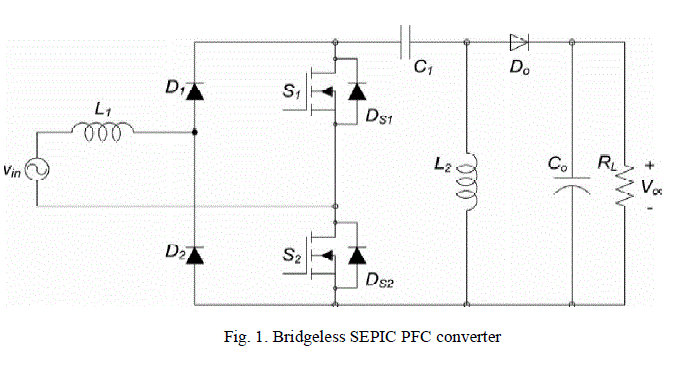
| In Fig. 1, a bridgeless SEPIC PFC converter suggested is shown. The component count is reduced and it shows high efficiency due to the absence of the full-bridge diode. However, in this converter, an input inductor with large inductance should be used in order to reduce the input current ripple. In addition, the conduction losses on intrinsic body diodes of the switches are caused by using single pulse width modulation (PWM) gate signal. |
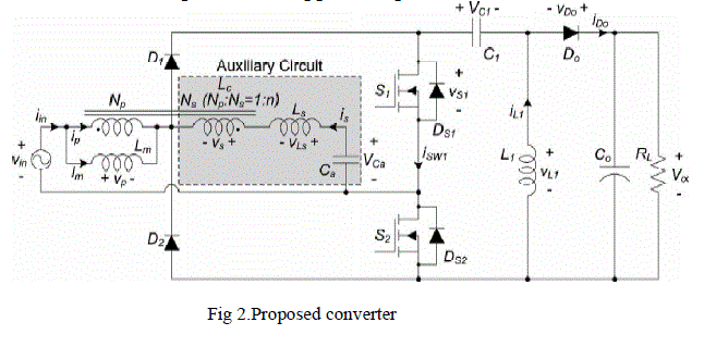
| In order to overcome these problems, a bridgeless SEPIC converter with ripple-free input current is proposed in Fig. 2.An auxiliary circuit, which consists of an additional winding of the input inductor, an auxiliary small inductor, and a capacitor, is utilized to reduce the input current ripple. Coupled inductors are often used to reduce current ripple. |
ANALYSIS OF THE PROPOSED CONVERTER
|
| The auxiliary circuit of the proposed converter includes an additional winding Ns of the input inductor Lc ,an auxiliary inductor Ls, and a capacitor Ca. The coupled inductor Lcis modeled as a magnetizing inductance Lm and an ideal transformer which has a turn ratio of 1:n(n=Ns /Np).The leakage inductance of the coupled inductor Lcis included in the auxiliary inductor Ls. The capacitance of Cais large enough, so Cacan be considered as a voltage source VCaduring a switching period. Since the average inductor voltage should be zero at a steady state according to the voltsecond balance law, the average capacitor voltage VCais equal to the input voltage vin during a switching period. Similarly, the average capacitor voltage VC1 is equal to vin . Diodes D1 and D2 are the input rectifiers and operate like a conventional SEPIC PFC converter. DS1 andDS2 are the intrinsic body diodes of the switches S1 and S2 . The switches S1 and S2 are operated with the proposed gate signals. The other components C1, L1,Do, and Co are similar to those of the conventional SEPIC PFC converter. |
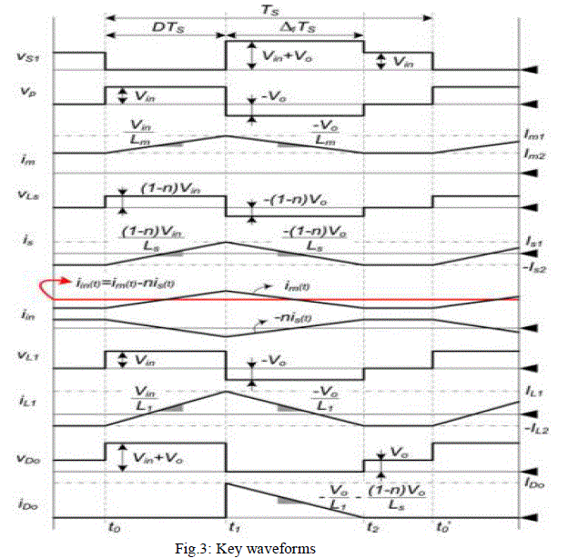
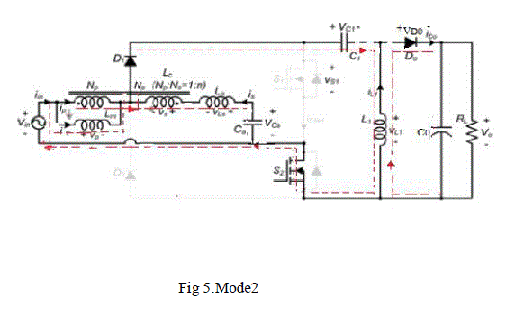
| It is assumed that the converter operates in discontinuous conduction mode (DCM). so the output diode Do is turned OFF before the main switch is turned ON. The capacitance of the output capacitor Co is assumed sufficiently large enough to consider the output voltage Voas constant. Also, the input voltage is assumed constant and equal to Vin in a switching period Ts. The operation of the proposed converter is symmetrical in two half-line cycles of input voltage. The operation of the proposed converter in one switching period Tscan be divided into three modes. Fig. 5 shows the operating modes in the positive input voltage. Before t0 , the switch S1 and the diode Do are turned OFF and the switch S2 is conducting. The input current is the sum of the freewheeling currents IS2 and IL2 . |
| Mode 1 [t0, t1 ] |
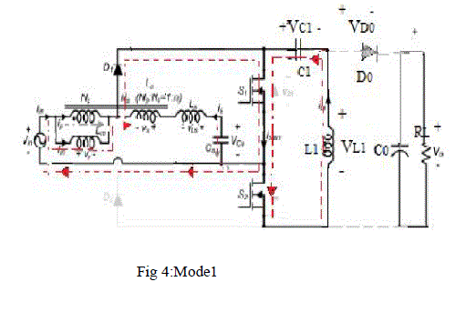
| At t0 , the switch S1 is turned ON and the switch S2 is still conducting. Since the voltage Vp across Lm is Vin, the magnetizing current im is increases from its minimum value. |
| Mode 2 [t1,t2] |
| In the mode 2 operation the switch S1 is turned OFF and the output diode D0 is conducting. The circuit diagram of mode 2 operation is shown in the Fig.5. At t1, the switch S1 is turned OFF and the switch S2 is still conducting. Since the voltage.Vp across Lm is −Vo, the magnetizing current im is decreases from its maximum value. |
| Mode 3 [t2,t0] |
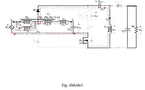
| In the mode 3 operations the switch S2 is conducting and the switch S1 is in turned OFF condition. The circuit diagram of mode 3 operation is shown in the Fig.6. The output diode is turned OFF during this mode of operation. At t2 , the current iDo becomes zero, and the diode Do is turned OFF. |
POWER FACTOR CORRECTION
|
| The most loads in modern electrical distribution systems are inductive there is an ongoing interest in improving powerfactor. The low power factor of inductive loads can adversely affect voltage level. As such, power factor correction throughthe application of capacitors is widely practiced at all system voltages. As utilities increase penalties they charge customers are highly efficient and fast in response. |
| A .Power factor improvement |
| In order to understand power factor, one must first know the process of energy storage in capacitors and inductive devices. As the voltage in A.C circuits varies sinusoidal, it alternately passes through zero and starts towards maximum voltage. During this time, the inductive device gives up energy from its electromagnetic field, and the capacitor stores energy in its electrostatic field. As the voltage passes through a maximum point and starts to decrease, the capacitor gives up energy and Amp-Reactive (KVAR)generator, since it actually a supplies magnetizing requirementsin the inductive device. The inductivedevice stores energy. Thus, when a capacitor and an inductivedevice are installed on the same circuit, there will be anexchange of magnetizing current between them, that is, theleading current taken by the capacitor neutralizes themagnetizing current to the inductive device. The capacitormay be considered to be a Kilo Volt.Amp-Reactive (KVAR)generator, since it actually a supplies magnetizing requirementsin the inductive device. |
| B. Power Factor Correction |
| The power factor correction method is improves theefficiency of the converter. Power factor correction is the method of correcting the power factor closer to one. Power factor correction is applied to different applications such as in: electrical power transmission utilities to improve the stability and efficiency of the transmission network. There are several advantages in utilizing power factor correction capacitors that is increased load carrying capabilities in the circuits, improved voltage and reduced power system losses. |
SIMULATION RESULTS OF BASIC BRIDGELESS PFC CIRCUIT
|
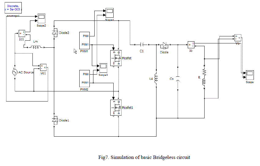
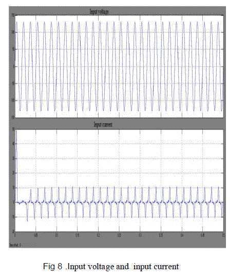
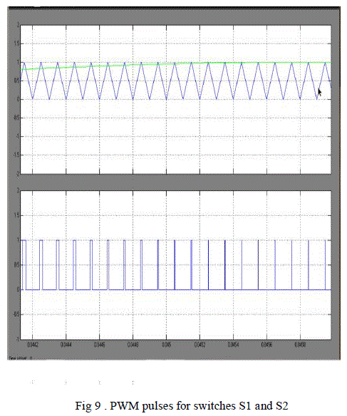
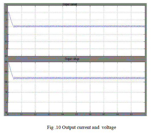
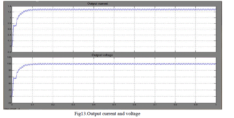
| The converter topology was simulated in the MATLAB/ SIMULINK software for validation of topology. Fig 8shows the input voltage and input current waveform. From the waveform we can see that the input current consists some ripples. This is a disadvantage of this circuit. Fig 9 shows the PWM pulses for the switches S1 and S2. Fig 10shows the output voltage and current waveform. |
SIMULATION OF PROPOSED BRIDGELESS SEPIC CONVERTER
|
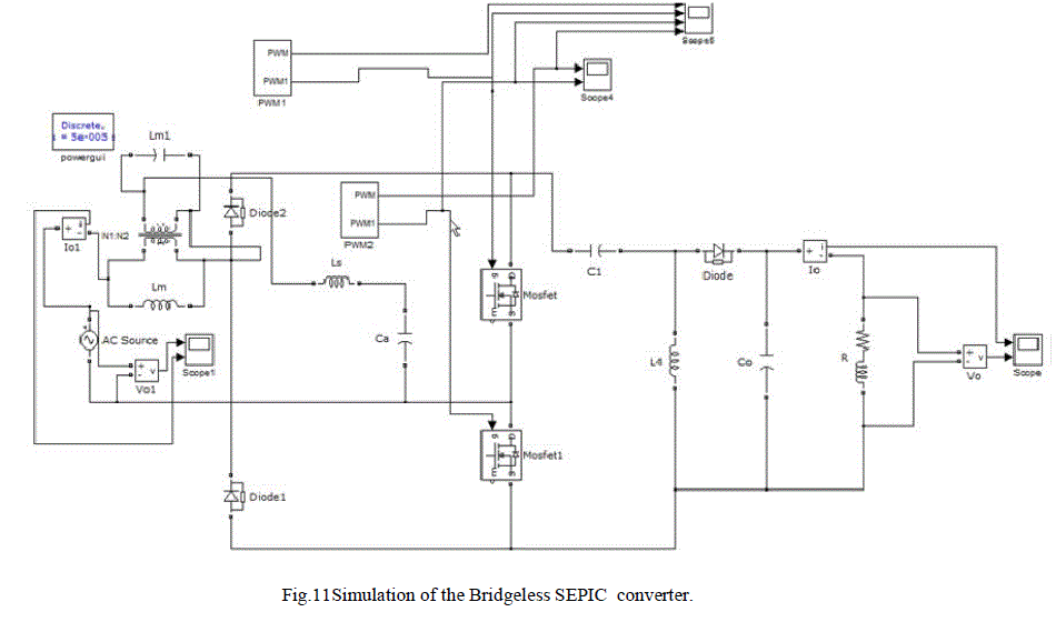
| The conventional Bridgeless SEPIC PFC converters contains some input current ripples.Inorder to overcome these problem, a Bridgeless SEPIC converter with ripple-free input current is proposed.In this converter, the input bridge diode is removed and the conduction losses reduced. The input current ripple is significantly reduced by utilizing an additionalwinding of the input inductor and an auxiliary capacitor.An auxiliary circuit, which consists of an additionalwinding of the input inductor, an auxiliary small inductor, and acapacitor, utilized to reduce the input current ripple.Coupled inductors are often used toreduce current ripple. |
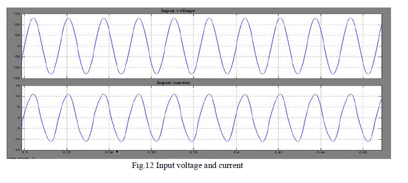
| The proposed converter is simulated by MATLAB/ SIMULINK. From the fig 12we can seethat the input current is a perfect replica of the input voltage and is exactly in phase withthat.The input current ripples are reduced by using the coupled inductors which has a small magnetizing inductance. |
SPEED AND TORQUE CONTROL OF DC MOTOR
|
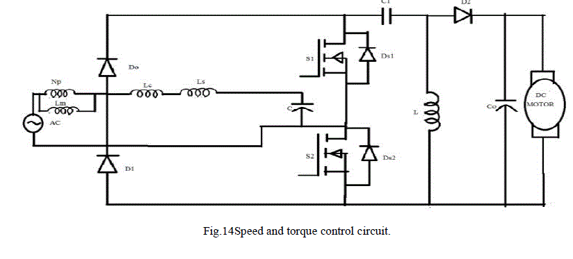
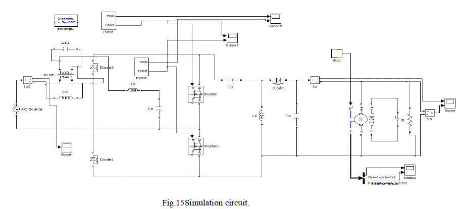
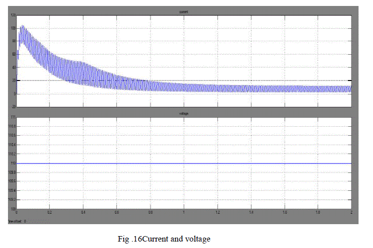
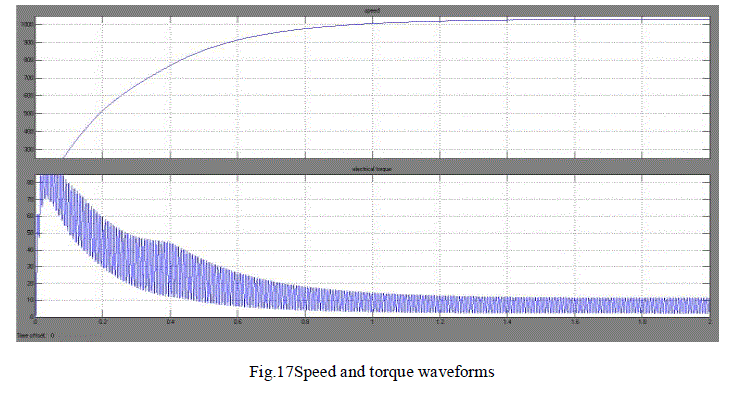
| In the proposed circuit the some output power is wasted as heat. So to avoid this heating losses, a DC motor connected across the output capacitor. So we can make the output power become useful. This DC motor can be connected to the cranes pulley, etc. We can vary the output voltage by varying the duty ratios. So by varying the output voltage ,speed and torque waveforms also varied. The circuit is simulated by MATLAB/ SIMULINK and plot the speed,torque,output voltageand output current waveforms. |
EXPERIMENTAL RESULTS
|
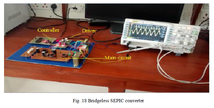
| The hardware set up of the proposed model was done with PIC 16F877A micro controller, and is shown in Fig 18. The hardware model consists of three main parts - Controller,circuit, Driver circuit and the main circuit diagram. In addition to these three, two 230/12 V transformers are also provided. One of the transformer is used to provide supply for the main circuit, where as the other transformer is to provide supply for the driver and controller circuit. |
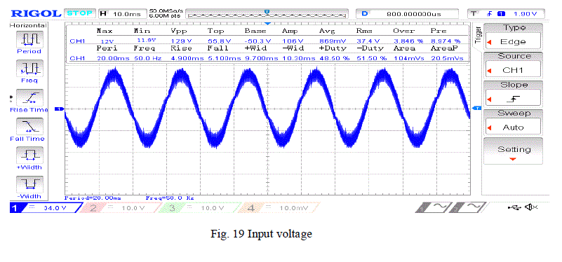
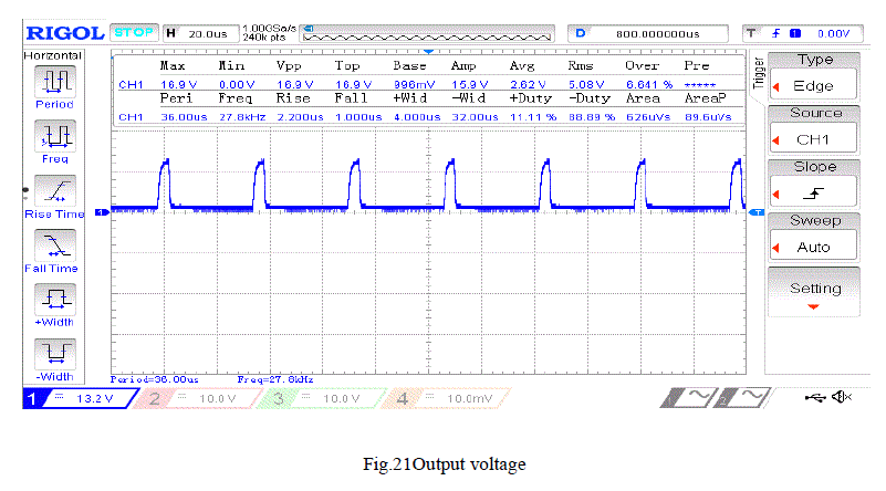
| Due to practical difficulties of making the hardware section speed control DC Motor, here a SEPIC converter with reduced conduction losses and switching losses with ripple free input current is experimentally verified. The output voltage is maintained at 7V with input voltage 12V,50Hz supply. |
CONCLUSION
|
| A bridgeless SEPIC converter with ripple-free input current has been proposed. In this converter the input full-bridge diode is eliminated. With the proposed gate driving method, the efficiency is improved. In this paper a Bridgeless SEPIC converter with reducedcomponents and low conduction losses is designed and used for the speed control of DC motor.It is designed to work in Discontinuous Conduction Mode (DCM). To achieve the speed control of DC motor by varying duty ratios. This converter is developed in MATLABsimulink and performance are verified. The hardware setup of the proposed model was done with PIC 16F877A microcontroller. The input current ripple of the proposed converter is significantly reduced by utilizing an auxiliary circuit consisting of an additional winding ofthe input inductor, an auxiliary small inductor, and a capacitor.The major disadvantage ofthe proposed converter is that it has three magnetic components |
Tables at a glance
|
 |
| Table 1 |
|
| |
Figures at a glance
|
 |
 |
 |
 |
 |
| Figure 1 |
Figure 2 |
Figure 3 |
Figure 4 |
Figure 5 |
 |
 |
 |
 |
| Figure 6 |
Figure 7 |
Figure 8 |
Figure 9 |
 |
 |
 |
 |
| Figure 10 |
Figure 11 |
Figure 12 |
Figure 13 |
 |
 |
 |
 |
| Figure 14 |
Figure 15 |
Figure 16 |
Figure 17 |
 |
 |
 |
 |
| Figure 18 |
Figure 19 |
Figure 20 |
Figure 21 |
|
| |
References
|
- Bridgeless SEPIC Converter With a Ripple-Free Input Current Jae-Won Yang and Hyun-Lark Do IEEE Trans on Power electronics, Vol. 28, No. 7, Jul 2013
- W.-Y. Choi, J.-M.Kwon, E.-H.Kim, J.-J.Lee, and B.-H. Kwon, Bridgeless boost rectifier with low conduction losses and reduced diode reverserecovery problems, IEEETrans. Ind. Electron., vol. 54, no. 2, pp. 769780, Apr. 2007.11471157, Apr. 2009.
- L. Huber, Y. Jang, and M. M. Jovanovic, Performance evaluation of bridgeless PFC boost rectifiers, IEEE Trans. Power Electron., vol. 23, no. 3, pp. 13811390, May 2008.
- H.-Y. Tsai, T.-H.Hsia, and D. Chen, A family of zero-voltage-transition bridgeless power-factor-correction circuits with a zero-current-switching auxiliary switch, IEEETrans. Ind. Electron., vol. 58, no. 5, pp. 1848 1855, May 2011.
- J. P. R. Balestero, F. L. Tofoli, R. C. Fernandes, G. V. Torrico-Bascope, and F. J. M.de Seixas, Power factor correction boost converter based on the three-state switching cell, IEEE Trans. Ind. Electron., vol. 59, no. 3, pp. 15651577, Mar. 2012.
- A. J. Sabzali, E. H. Ismail, M. A. Al-Sa_ar, and A. A. Fardoun, New bridgeless DCM SEPIC and CUK PFC recti_ers with low conduction and switching losses, IEEE Trans.Ind. Appl., vol. 47, no. 2, pp. 873881, Mar./Apr. 2011.
- H. -L. Do, Soft-switching SEPIC converter with ripple-free input current, IEEE Trans. Power Electron., vol. 27, no. 6, pp. 28792887, Jun. 2012.rs, IEEE Trans. Power Elec- tron., vol. 26, no. 2, pp. 541550,
- X. Margueron, and N. Idir, High-frequency model of the coupled inductors used in EMI filters, IEEE Trans. Power Electron., vol. 27, no. 6, pp. 28052812, Jun. 2012.
- B. Su and Z. Lu, An interleaved totem-pole boost bridgeless rectifier with reduced reverse-recovery problems for power factor correction, IEEE Trans. Power Electron., vol. 25, no. 6, pp. 14061415, Jun. 2010
- Y. Zhao, W. Li, Y. Deng, and X. He, Analysis, design, and experimentation of an isolated ZVT boost converter with coupled inductors, IEEE Trans. Power Electron., vol. 26, no. 2, pp. 541550, Feb. 2011
- W. Wang, D. D.-C. Lu, and G. M.-L. Chu, Digital control of bridgeless buck PFC converter in discontinuous-input-voltage-mode, in Proc. Annu.Conf. IEEE Ind. Electro. Society, 2011, pp. 13121317.
- Y.W. Lo and R.J. King, "High performance ripple feedback for the buck unity-power- factor rectifier," IEEE Transactions on Power Electronics, vol. 10, no.2, pp.158-163, March 1995.39
|