Keywords
|
| UPS, QZSI, CQZSI, MOSFET, SPWM, VSI, PWM, THD. |
INTRODUCTION
|
| The voltage fed quasi z source inverter is derived from the Z source inverter. It includes all the advantages of Z source inverter like voltage buck and boost operation. Here, the input source is obtained from various sources like Fuel cell, Solar panel and UPS. This source voltages can be varied based on its condition [1-7-11-13].If necessary, the QZSI can be operates at shoot through mode, which is the conduction of two switches in same phase leg or all the switches in the inverter. This shoot through mode is not applicable in VSI because it causes short circuit and makes damage in the circuit. In QZSI, shoot through mode is used to boost the magnetic energy storage in dc side inductors like L1 and L2 without making the short circuit in the capacitors C1 and C2. This kind of magnetic storage provides the boost voltages at the inverter output during operating states. If the input voltage is more than the enough means, the shoot through modes are terminated, and it could be operates as a nominal VSI and it gives a constant output at the inverter output. This paper discusses a performance improvement of voltage-fed quasi Z source inverter by introducing the cascaded quasi Z source inverter. This cascaded quasi Z source inverter can be derived from the quasi Z source inverter by adding of one diode (D2), one inductor (L3) and two capacitors (C3 and C4), as shown in Fig. 1(b). The cascaded quasi Z source inverter duty cycle period for shoot through state is decreased at the same voltage boost factor and the stress for the components also reduced, when it is compared to the quasi Z source inverter [2-3-12]. Because of reduced shoot through duty cycle, the values of inductors and capacitors of CQZSI are decreased than the QZSI. At the same time, for the same component ratings, voltage and current stress, the cascaded quasi Z source inverter should gives a high voltage boost factor. |
| Fig. 1 shows the block diagram of cascaded quasi Z source inverter. In this, the dc voltage from the source is fed into the cascaded quasi Z source inverter, it could boost the input voltage and the boosted voltage is fed into the three phase inverter. The three phase inverter converts the input dc voltage into an ac voltage in the output side; this could be done by the switches in the inverter. The switches can be controlled by using sinusoidal pulse width modulation. This CQZSI can be operates at two different operating conditions. Here, the MOSFET can be used as switches in the inverter. |
| Fig. 2 contains both voltage fed QZSI and voltage fed CQZSI along with LC filter in the output side. The LC filter can be used to eliminate the unwanted signal present in the output side, the inductor is placed in series to the phase and the capacitor is connected in parallel between the phases. |
RELATED WORK
|
| In the existing Quasi Z source inverter, the output voltage can be increased or decreased from the various input voltage based on its applications. In this the period of shoot through duty cycle is high, so it causes voltage stress in the inverter switches to makes the system as failure. To avoid the system failure, the shoot through duty cycle period must reduce. It could be done by adding of one diode (D2), one inductor (L3) and two capacitors (C3 and C4) to the existing system. By making this arrangement, the shoot through duty cycle can be reduced up to 30% for the same boosting factor. |
DESCRIPTION OF CASCADED QUASI Z SOURCE INVERTER
|
| The voltage from the sources can be fed into the cascaded quasi Z source network, then the dc voltage from the network is converted into an ac voltage by using an inverter [4-6]. Here, two different modes of operations can be done because of varying input voltage. The two different operating modes are: shoot-through and non-shoot-through mode. In the non-shoot-through mode, the cascaded quasi Z source inverter performs only the voltage buck function. This kind of mode is mostly used at light load condition, when the input voltage is more than the nominal input. The inverter can be controlled as same as VSI, and it could utilize only the active states as only one switch is conducts in a phase leg. The switches can be controlled by using a sinusoidal pulse width modulation (SPWM). |
| A. Sinusoidal Pulse Width Modulation |
| Here sinusoidal pulse width modulation can be used for pulse generation for the switches. Triangular wave acts a carrier wave and sine wave can be used as a reference wave. The magnitude of reference wave is less than the carrier wave. If the reference wave is higher than the carrier wave means, the pulse can be generated. Here I am using a three phase inverter, so i want generate a three different pulses from three phase reference sine wave with the carrier triangular wave. Each sine wave is 1200 phase shift [8]. This three phase sine wave should have same magnitude but this magnitude is less than the carrier wave magnitude. Pulse generated from phase A along with carrier wave is given to the switches T1 & T2, from the phase B along with carrier wave generated pulse given to the switches T3 & T4, from the phase C along with carrier wave generated pulse given to the switches T5 & T6. For example, the carrier wave amplitude is 1 means; the amplitude of reference wave is 0.7. Because, the reference wave amplitude is always lesser than the carrier wave amplitude. |
| When the input voltage drops from the defined value means, the CQZSI starts to operate at the shoot-through mode. To boost the input voltage, a special shoot-through mode is implemented by using a sinusoidal pulse width modulation [5].During this mode; the load can be shorted through all switches. This type of shoot-through mode is forbidden in VSI. |
| The shoot-through state is possible in cascaded quasi Z source inverter effectively; it doesn’t cause any short circuit and protecting the circuit from damage [9-10]. This shoot through mode is used to boost the magnetic energy storage in dc side inductors like L1 and L2 without making the short circuit in the capacitors C1 and C2. This kind of magnetic storage provides the boost voltages at the inverter output during operating states. |
| B. PWM Techniques |
| There are several PWM techniques available for cascaded quasi Z- source inverter. In this, the technique can be varied by changing the modulation index. The PWM method for cascaded quasi Z-source inverter is given below: |
| 1. Simple boost |
| 2. Maximum boost |
| 3. Maximum constant boost |
| 4. 3rd harmonic control boost |
| The advantages of using PWM techniques are: |
| 1. The output voltage control by this method can be obtained without any additional components. |
| 2. Lower order harmonics can be eliminated or minimized along with its output voltage control. As higher order harmonics can be filtered easily, the filtering requirements are minimized as higher order harmonics can be filtered easily. |
| 3. The biggest advantage for controlling power with PWM is heat management. The power transistors are either fully on (nearly zero volts drop) or fully off (zero current). So in both conditions a transistor doesn't dissipate much heat (power). Equipment stays cool, no big heat sinks. Also transistors only need to be rated for maximum current and voltage, because the power will always be fine. |
CIRCUIT ANALYSIS OF CASCADED QUASI Z SOURCE INVERTER
|
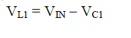
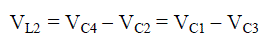
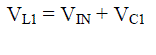
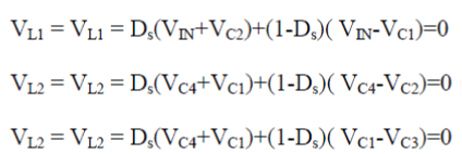
| In the non-shoot-through mode, the inverter bridge seen from the source is equivalent to a current source [Fig. 4(a)]. From Fig. 4(a), for the active states, the inductors voltage can be represented as |
 |
 |
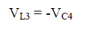 |
| In the shoot-through state [Fig. 4(b)], the inductors voltages can be represented as |
 |
 |
 |
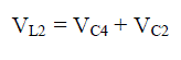
| The duty cycles of the shoot-through and non-shoot-through states are considered as Ds and (1-Ds). At steady state, the average inductors voltages over one switching period are zero. |
 |
 |
| From (1)–(7), we obtain |
 |
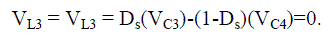 |
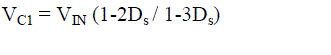
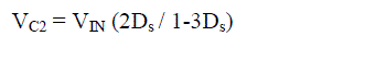
| Solving (8), the capacitors voltages of C1…….C4 could be found as, |
 |
 |
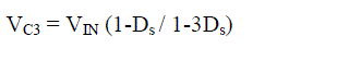 |
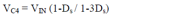 |
| In this analysis of cascaded quasi Z source inverter, the output can be varied depends on the varying boosting condition. Here, there are various types of boosting can be made as like simple boost, constant boost, and 3rd order harmonics. The period of shoot-through is varied based on the boosting condition, and the magnitude of reference wave and carrier wave also gets varied. The shoot-through mode pulses can be generated by the constant dc voltage is given as the reference wave along with the reference sine wave. This magnitude should be higher than the reference sine wave but lesser than the carrier triangular wave. Pulse generated from both reference wave is combined by using an OR gate, makes as a single pulses. This pulse can be given to the switches, it could makes the switches to conduct at the same phase leg during the both pulses from constant dc voltage and sine wave should be at maximum condition. |
| The CQZS-network reduces up to 33.3% in the shoot-through duty cycle at the same input voltage boost factor. The inductors and capacitors values of the CQZS-network could also be reduced in comparison with the quasi Z source inverter. But, the number of passive components and their summarized values will be increased. The output voltage and current for both line and phase are measured, along with this THD values can also be measured by using MATLAB/ Simulink. |
| Fig. 6(a) shows the output line voltage & current waveform of CQZSI. The output voltage Vrms=383V obtained at same input DC. Fig. 12 shows the output line voltage THD Value of CQZSI. Boost factor is 3.5 times of input voltage and its modulation index is 0.5. Fig. 6(c) shows the output line voltage waveform of CQZSI. The output voltage Vrms=415V is obtained from 95V input DC. Fig. 6(e) shows the output line voltage THD Value of CQZSI. Boost factor is 4 times of input voltage and its modulation index is 0.7. Fig. 15 shows the output line voltage & current waveform of CQZSI. The output voltage Vrms=415V obtained at same input DC. Fig. 16 shows the output line voltage THD Value of CQZSI. Boost factor is 4 times of input voltage and its modulation index is 0.5.And I added 3rd order harmonics with each reference wave for generating the reference wave. |
CONCLUSION
|
| In this paper cascaded quasi Z source inverter can be analysed by using various Sinusoidal Pulse Width Modulation techniques as like constant boost, simple boost and 3rd harmonic pulse generation. And it can vary based on its application. Moreover, the cascaded quasi Z source inverter reduced the shoot through duty cycle by over 30% at the same voltage boost factor and the components stress can be reduced. |
| Here, line voltage and phase voltage along with THD analysis can be done at different boosting conditions. And those outputs can be shown in the previous chapter. The boosting factor of cascaded quasi Z source inverter is 4 times of input voltage at constant boost. Those simulation output can be simulated by using MATLAB simulation. To further decrease the shoot through duty cycle at the same voltage boost factor, the number of stages of the quasi Z source inverter could be increased. It contains all the advantages of quasi Z source inverter and it is high reliability. |
Figures at a glance
|
 |
 |
 |
| Figure 1 |
Figure 2 |
Figure 3 |
 |
 |
 |
| Figure 4 |
Figure 5 |
Figure 6 |
|
| |
References
|
- Anderson.J and Peng F. Z., “Four quasi-Z-source inverters,” in Proc. IEEE Power Electron. Spec. Conf., pp. 2743–2749, Jun. 15–19, 2008.
- Gajanayake .J, H. B. Gooi, F. L. Luo, P. L. So, L. K. Siow, and Q. N. Vo, “Simple modulation and control method for new extended boost quasi Z-source inverters,” in Proc. IEEE Region 10 Conf. (TENCON, pp. 1–6), Jan. 23–26, 2009.
- Gajanayake.J, F. L. Luo, H. B. Gooi, P. L. So, and L. K. Siow, “Extended-boost Z-source inverters,” IEEE Trans. Power Electron., vol. 25, no. 10, pp. 2642–2652, Oct. 2010.
- Kwon.J.-M, E.-H. Kim, B.-H. Kwon, and K.-H. Nam, “High-efficiency fuel cell power conditioning system with input current ripple reduction,”IEEE Trans. Ind. Electron., vol. 56, no. 3, pp. 826–834, Mar. 2009.
- Lee.W.-J, C.-E. Kim, G.-W. Moon, and S.-K. Han, “A new phase shifted full-bridge converter with voltage-doubler-type rectifier for high efficiency PDP sustaining power module,” IEEE Trans. Ind. Electron., vol. 55, no. 6, pp. 2450–2458, Jun. 2008.
- Li.Y, Anderson.J, F. Z. Peng, and D. Liu, “Quasi-Z-source inverter for photovoltaic power generation systems,” in Proc. IEEE APEC, pp. 918–924, Feb. 15–19, 2009.
- Park J.-H., H.-G. Kim, E.-C. Nho, T.-W. Chun, and J. Choi, “Gridconnected PV system is using a quasi-Z-source inverter,” in Proc. IEEE APEC, pp. 925–929, Feb. 15–19, 2009.
- Roasto and D. Vinnikov, “Analysis and evaluation of PWM and PSM shoot-through control methods for voltage-fed QZSI based DC/DC converters,” in Proc. 14th Int. EPE-PEMC, pp. T3-100–T3-105, Sep. 6–8, 2010.
- Vaisanen.V, T. Riipinen, and P. Silventoinen, “Effects of switching asymmetry on an isolated full-bridge boost converter,” IEEE Trans. Power Electron., vol. 25, no. 8, pp. 2033–2044, Aug. 2010.
- Vinnikov, I. Roasto, R. Strzelecki, and M. Adamowicz, “CCM and DCM operation analysis of cascaded quasi-Z-source inverter,” in Proc. IEEE ISIE, pp. 159–164, Jun. 27–30, 2011.
- Vinnikov, I. Roasto, R. Strzelecki, and M. Adamowicz, “Two-stage quasi-Z-source network based step-up DC/DC converter,” in Proc. IEEEISIE, pp. 1143–1148, Jul. 4–7, 2010.
- Vinnikov.D, I. Roasto, R. Strzelecki, and M. Adamowicz, “Performance improvement method for the voltage-fed QZSI with continuous input current,” in Proc. 15th IEEE MELECON, pp. 1459–1464, Apr. 26–28, 2010.
- Vinnikov .D and I. Roasto, “Quasi-Z-source-based isolated dc/dc converters for distributed power generation,” IEEE Trans. Ind. Electron., vol. 58, no. 1, pp. 192–201, Jan. 2011.
|