Keywords
|
| CMOS VCO, Current-Starved VCO,LT SPICE IV |
INTRODUCTION
|
| A voltage controlled oscillator (VCO) is one of the most important basic building blocks in analog and digital circuits. In a wireless system the quality of the communication link is determined in large part by the characteristics of the VCO and in today’s wireless communication systems greater frequency range is required by the VCOs. Traditionally, VCOs using CMOS technology have been used for low frequency applications, but submicron processes have allowed CMOS oscillators to achieve frequencies in the gigahertz range [2]. This range is made possible with the use of automatic swing control. VCO can be built using many circuit techniques [5]. In this paper designing of CMOS VCO using LT spice here current starved VCO is design. Though there are so many design requirements of a VCO, which are phase stability, large electrical tuning range, linearity of frequency verses control voltage, large gain factor, capability of accepting wideband modulation and low cost but the most important factor in designing the VCO is the linearity, on the basis of which the comparison between CMOS VCOs is described [6]. With respect to digital phones that use these circuits, low power consumption, small size and low fabrication costs are important design factors. |
CURRENT STARVED VCO
|
| A ring oscillator is comprised of a number of delay stages, with the output of the last stage fed back to the input of the first. To achieve oscillation, the ring must provide a phase shift of 2π and have unity voltage gain at the oscillation frequency. This current starved VCO is designed using ring oscillator and its operation is also similar to that. From the schematic circuit shown in the Figure 1, it is observed that MOSFETs M2 and M3 operate as an inverter, while MOSFETs M1 and M4 operate as current sources. The current sources, M1 and M4, limit the current available to the inverter, M2 and M3; in other words, the inverter is starved for the current. The MOSFETs M5 and M6 drain currents are the same and are set by input control voltage. The currents in M5 and M6 are mirrored in each inverter/current source stage. The upper PMOS transistors are connected to the gate of M6 and source voltage is applied to the gates of all lower NMOS transistors [4]. |
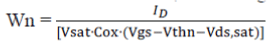
| The drain current of a short channel MOSFET operating in saturation region is given by: |
 |
| From this equation we can write the equation for the width of NMOS, which is given by: |
 |
| Now, BSIM4 MOSFET model Parameters are: |
| By putting the values of these parameters in the equation of Wn, we get the value Wn in 45nm technology, which is given by: |
| Wn = 180nm |
| For the Ratio of W/L, |
| (W/L) p = 2.5(W/L) n |
| Now, we know that the values of L for NMOS and PMOS are same in 45 nm technology, so we get |
| Lp = Ln = 45nm |
| So, the ratio will be |
| Wp = 2.5Wn |
| By putting the values of Wn in above equation, we get |
| Wp = 450nm |
| Finally we get the ratio of W/L for NMOS & PMOS in 45nm technology: |
| ? For NMOS: Wn = 180nm, Ln = 45nm. |
| ? For PMOS: Wp = 450nm, Lp = 45nm |
DESIGN OF VCO
|
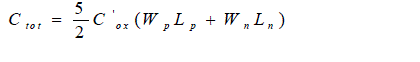
| To determine the design equations for use with the current-starved VCO, the total capacitance on the drains of M2 and M3 is given by |
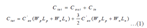 |
| This is simply the output and input capacitances of the inverter. The equation can be written in more useful form as |
 |
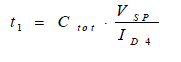
| The time it takes to charge t o t C from zero to S P V with the constant current D 4 I is given by |
 |
| While the time it takes to discharge tot C from VDD to SP V is given by |
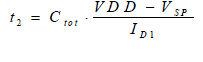 |
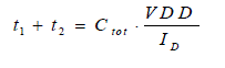
| If D 4 I = D 1 I = D I (which is labelled as D c e n t e r I when i n V C O V = VDD/2), then the sum of 1 t and 2 t is simply |
 |
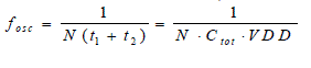
| The oscillation frequency of the current starved VCO for N (an odd number >= 5) of stages is |
 |
| The centre frequency (f centre) of the VCO when D I = D c e n te r I . The VCO stops oscillating, neglecting sub-threshold currents, when in V C O V < TH N V . Therefore, min V = TH N V and m in f = 0. |
| The maximum VCO oscillation frequency, m ax f , is determined by finding D I when in V C O V = VDD. At the maximum frequency, m a x V = VDD. |
| The output of the current starved VCO normally has its output buffered through one or two inverters. Attaching a large load capacitance on the output of the VCO can significantly affect the oscillation frequency or lower the gain of the oscillator enough to kill oscillations altogether. |
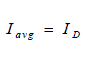
| The average current drawn by the VCO is |
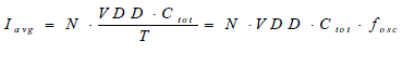 |
| Or |
 |
| The average power dissipated by the VCO is |
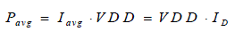 |
| If the power dissipated by the mirror MOSFETs, M5 and M6, is also included then the power is doubled from that given by the equation (9), assuming that D D 5 D 6 . For low power dissipation D I should be kept low, or in other words oscillation frequency should be low [4]. |
| We begin by calculating the total capacitance Ctot. Using equation and assuming the inverters, M2 and M3, are sized for equal drive, that is, Ln = Lp = 1, |
| Wn = 10 and Wp =20, the capacitance is |
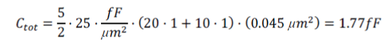 |
| Let’s use a centre drain current of 10μA based on ID - VGS characteristics of the MOSFETs. The selection of the current is important because when VinVCO is VDD/2, the oscillation frequency to be 1GHz. The oscillation frequency of the current-starved VCO for N of stages is given by [2] |
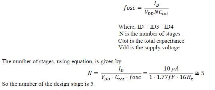 |
SIMULATION RESULT OF CURRENT STARVED VCO
|
| Functional simulation Of Current Starved VCO is done In LT-Spice software using 45 nm CMOS technology. The five stage CSVCO implementation is shown in figure 2.There are two number of buffers .The tuning range of VCO is from 8Mhz to 7346Mhz.The simulation result of current starved VCO of 5 stage is shown 3. |
| When we apply control voltage of 0.42v then we get output waveform of central frequency 1Ghz sown in fig 3.Similarly for different control voltage we get different oscillation frequency range from 8 MHz to 7346 MHz is shown in table 2. |
CONCLUSION
|
| In this paper we observed that in current starved voltage controlled oscillator (VCO) generates 1GHz frequency at input control voltage (VinVCO) of 420mV. Since Phase locked loop (PLL) is widely used in wireless communication systems, hence we can generate any desire frequency based on application requirements.The comparative analysis of csvco with the reference paper is show. |
Figures at a glance
|
 |
 |
 |
| Figure 1 |
Figure 2 |
Figure 3 |
|
| |
References
|
- B. Razavi, “Monolithic phase-locked loops and clock recovery circuits- theory and design”, IEEE Press,pp. 283-377 and 381-483, 1996.
- M. Banu, “MOS oscillators with multi-decade tuning range and gigahertz maximum speed”, IEEE Journal of Solid-State Circuits, vol. 23, pp. 1386–1393, December 1988.
- D. A. Hodges and H.G. Jackson, “Analysis and design of Digital Integrated Circuits”,2nd edition, McGraw-Hill, 1988.
- R. Jacob Baker, Harry W. Li and David E. Boyce, “CMOS Circuit Design, Layout and Simulation,” IEEE Press Series on Microelectronics Systems, pp. 355-361 and383-387, 2000.
- M. Jamal Deen, “Ultra Low-Voltage Low-Power Voltage Controlled Oscillator”, Electrical and Computer Engineering Department, CRL 226 McMaster University, Hamilton, ON, Canada L8S 4K1.
- M. J. Underhill, “Fundamentals of oscillator performance”, Electronics and Communication Engineering Journal, vol. 4, no. 4, pp. 185-193, 1992.
- Paul R. Gray and Robert G. Meyer, “Analysis and Design of Analog Integrated Circuits”, 3rd edition, John Wiley, January 1993.
- B. P. Panda, p. K. Rout, d. P. Acharya and g. Panda “Design of a novel current starved VCO via constrained geometric programming” april 12- 14 2011 international symposium on devices mems intelligent systems communications 2011.
|