Keywords
|
| Carry-Look ahead Adder (CLA) Block, HDL Languages, Xilinx ISE Simulator. |
INTRODUCTION
|
| Fast addition is an essential arithmetic function for most advanced digital systems. It heavily impacts the overall performance of digital systems. Various adder structures can be used to execute addition, such as serial and parallel structures. Most research works of adders are focused on the design of high-speed, low-area, or low-power adders. Recently, design of reconfigurable adders has received significant attentions. Reconfigurable adders usually are employed to achieve real-time processing of media signals. Moreover, future systems will shift toward more programmable and reconfigurable integrated system on chips (SOCs)[13].Thus fast and reconfigurable adders for arithmetic computing are needed. In past, the major challenge for VLSI designer is to reduce area of chip by using efficient optimization techniques and then the next phase is to increase the speed of the operation to achieve fast calculations. Arithmetic logic unit is the main component of central processing unit, where the addition, multiplication, comparison and other logical operations are performed. There are lots of research going on to the reduce power consumption in VLSI circuits. The PowerPC microprocessor has a reconfigurable ripple carry adder using additional bits for partitioning, such that multiple smaller adders are obtained. For example, the Add/Compare block of the microprocessor can execute separate 8-bit, 16-bit, and 32- bit additions with a 36-bit reconfigurable adder. The adder has four 9-bit segments and each segment consists of 8-bit operand data and an additional partition bit. Each partition bit determines that the carry of the corresponding segment addition is blocked or propagated. |
| There are three performance parameter on which a VLSI designer has to optimize their design, which are Area, Speed, and Power. Moreover, There are various types of adders such as Ripple Carry Adder (RCA), Shannon Adder(SA),Carry-Look ahead Adder (CLA), Carry Save Adder (CSA), Carry Select Adder, Carry-Bypass Adder or Carry Skip Adder (CSK) discussed [2]. |
A. Ripple Carry Adder(RCA)
|
| The Ripple carry adder is constructed by using cascading full adder(FA) blocks in series. The basic computation elements is a full adder(FA).It accepts three binary inputs A,B and Cin called addend, augends and carry in respectively the two outputs are the sum and the carry-out(Cout).A RCA is built by connecting the full adder, So that the carry out from each full adder is the carry –out from each full-adder is the carry-in to the next stages, the sum and carry bits are generated sequentially starting from the LSB, the Speed of the RCA is determined by the carry propagating time. The main advantages of this RCA are low power consumption and compact layout design smaller chip area [2]. |
B. Carry Lookahead Adder (CLA)
|
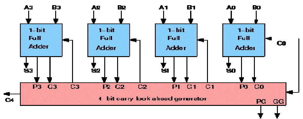
| Carry lookahead-adder is designed to eliminate the ripple carry delay and to overcome the latency introduced by the rippling effect of the carry bits [1]. This method based on the carry generating and the carry propagating functions of the full adder. This adder is based on the principle of looking at the lower bits of the augends and addend if a higher order is generated. This adder reduces the carry delay by reducing the number of gates through which a carry signal must propagate [2]. |
C. Carry Save Adder (CSA)
|
| The carry-save adder reduces the addition of 3 numbers to the addition of 2 numbers. The carry-save unit consists of ‘n’ full adders, each of which computes a single sum and carries bit based on the corresponding bits of the three inputs numbers. The entire sum can then be computed by shifting the carry sequence left by one place and appending a 0 to the front of the partial sum sequence and adding this sequence with RCA produces the resulting n+ 1 bit values applied in the partial product line of array multipliers will speed up the carry propagation in the array [2]. |
D. Carry Select Adder (CSLA)
|
| To solve the carry propagation delay, CSLA is developed which drastically reduces the area and delay to a great extent. The CSLA is used in many computational systems design to moderate the problem of carry propagation delay by independently generating multiple carries and then select a carry to generate the sum. It uses independent ripple carry adders (for Cin=0 and Cin=1) to generate the resultant sum. The final sum and carry are selected by the multiplexers (mux). A carry-select adder speeds faster than RCA by performing additions in parallel and reducing the maximum carry path. Because of the simulation technique the required area and power consumption of this adder is particularly doubles with respect to RCA [2]. |
E. Carry Skip Adder (CSkA)
|
| A carry-Skip consists of a simple ripple carry-adder with a special up carry chain called a skip chain. Carry skip adder is a fast adder compared to ripple carry adder. A carry-skip adder is designed to speed up a wide adder by aiding the propagation of a carry bit around a portion of the entire adder. However the industrial demands nowadays, which most desktop computers use word lengths of 32-bits like multimedia processors, makes the carry skip structure more interesting. These adders have different performance in terms of delay, area and power for same length of binary numbers. [2] |
| The paper is organized as follows: section II provides the overview of CLA adder, different section of CLA adder and its functioning. Section III presents the simulation results along with device utilization summary following with conclusion. |
F. Shannon Adder(SA)
|
| According to this theorem any logic expression is divided into two terms. One with a particular variable set to 1 and multiplying it by a variable and then set the variable to 0 and multiplying it by the inverse. The fullest reduction can be obtained by continuously repeating the Shannon theorem. This method is useful especially to multiplier and pass transistor circuit design. The Shannon’s theorem in a generalized way can be stated as a function of many variables, y (b0, b1,b2, y, bi, y, bn) can be written as the sum of two terms, say one with a particular variable ai , set to 0, and one with it set to 1. y (b0, b1, b2, ......bi,.....y, bn) = bi’y (b0, b1, b2, ......,0,.....y, bn) + bi y (b0, b1, b2, ......, 1,.....y, bn). |
| Shannon’s theorem is applied to the logical function using n-1 variables as control inputs and three data lines set to a logical ‘1’. These source inputs are then connected to the VDD lines (logical ‘0’), which are connected to the ground. The remaining nth variable is connected from the data input to the source input. The data signals flow horizontally and the control signals flows vertically. Remove pairs of transistors when they cancel each other. The Shannon expression output depends upon the pass logic ‘1’ or logic ‘0’. If it has logic’0’ then the connection input is given by 0 and by‘1’ for the connection input ‘1’. |
OVERVIEW OF CARRY LOOK-AHEAD ADDER
|
| Most of fast adders are based on being able to calculate the carry propagation much faster without having to wait for it to ripple through each bit of the adders. The carry look ahead technique is the most commonly used scheme for accelerating carry propagation. To compute a sum, An RCA requires in the worst case, n stage-propagation delays. For high speed processors, this scheme is undesirable. One way to improve adder performance is to use parallel processing in computing the carries. That is why Carry- look ahead adders are introduced [4] [5]. The carry-look ahead adder calculates one or more carry bits before the sum calculates, Due to this reduces the delay time to calculate the result of the larger number of value bits. |
| Let Ai and Bi be the I bits of the input data and Ci-1 the carry-in for stage i. the usual method computing the carryout Ci is |
 |
| Where The generate 'Gi ' in a full adder is given by |
 |
 |
 |
| The sum is generated by |
 |
| It is clear that the carry propagation delay is still long if the number of operands is large. Multilevel CLA networks can be used to cope with this problem by breaking the entire length of the operands into smaller blocks. That is, we may divide the stages into blocks and have a separate carry lookahead in each block. Then we may further reduce the delay of carry propagation by providing a carry-lookahead over blocks in addition to the internal lookahead with in the block. |
SIMULATION RESULTS
|
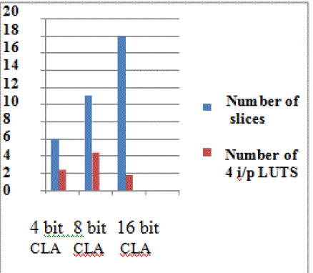
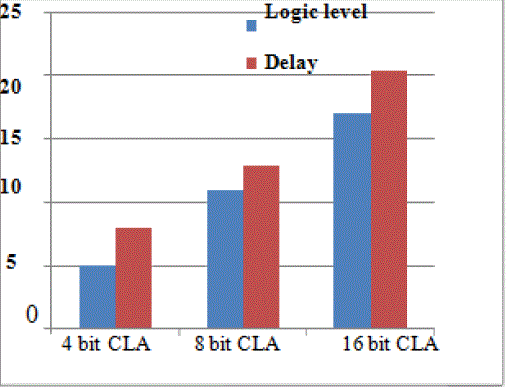
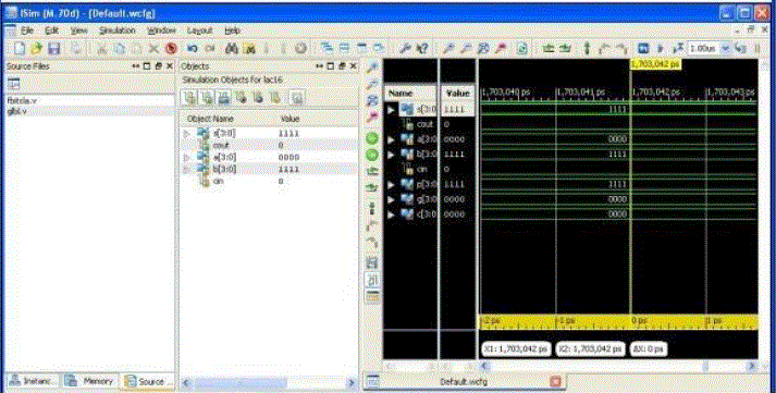
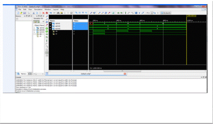
| This section presents the simulated results of different bits of carry look ahead adder. The different bits carry look ahead adder simulation was carried out using the Xilinx software. In every design circuit compulsory to check the design circuits works with required specification. The design is simulated at different bit levels by using Xilinx 12.1 Simulation results show that different bits are simulated so power consumption and propagation delay is varied. |
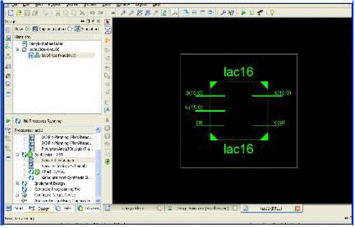
| Once you have simulated the code and synthesised it. Elaborate the RTL by double clicking on the lac module and you can notice that there will be exactly 16 lac module generated. |
| Here is the code for 4 bit Ripple Carry Adder using basic logic gates such as AND,XOR,ORetc.The module has two 4, 16 bit inputs which has to be added, and one 4,16-bit output which is the sum of the given numbers.Another output bit indicates whether there is a overflow in the addition, that means whether a carry is generated or not. |
CONCLUSION
|
| This paper has presented a design methodology of reconfigurable CLAs. A DFR scheme has proposed to divide a large CLA into multiple separate small ones. The DFR scheme only incurs a small amount of delay and area Penalty.We studied about different bits of adders theoretically as well as practically and by implementation and among compared them by different measures like Area, Delay and then Area- Delay Product. Comparing the performance metrics of adders for different word lengths using Verilog [3] and Xilinx as synthesis tool, The Carry Look Ahead Adder had the least Area-Delay product [4]. It is suitable for situations where both low power and fastness application places. To use the CLA in constant delay for the wider-bit adders it is not possible, since there will be a substantial loading capacitance, and larger delay and larger power consumption. |
Tables at a glance
|
 |
| Table 1 |
|
| |
Figures at a glance
|
 |
 |
 |
| Figure 1 |
Figure 2 |
Figure 3 |
 |
 |
 |
| Figure 4 |
Figure 5 |
Figure 6 |
|
| |
References
|
- Rajender Kumar, Sandeep Dahiya, “Performance Analysis of Different Bit Carry Look Ahead Adder Using VHDL Environment”International Journal of Engineering Science and Innovative Technology (IJESIT) Volume 2, Issue 4, July 2013
- S. Knowles, “A Family of Adders,” Proc. 15th IEEE Symposium onComputer Arithmetic, pp 277-281, 2001.
- Nazieh M. Botros, “HDL programming (VHDL and Verilog)”, Dreamtech Press (Available through John Wiley- India and ThomsonLearning) 2006 Edition.
- Jin-Fu Li, Jiunn-Der Yu, and Yu-Jen Huang, “A Design Methodology for Hybrid Carry- Lookahead/Carry-Select Adders withReconfigurability”, IEEE International Symposium on Circuits and Systems (ISCAS 2005), 23-26, May 2005.
- G.A.Ruiz, M.granda,”An Area –Efficient Staic Cmos Carry-Select Adder Based On A Compact Carry-Look Ahead Unit”.Microeletronic Journal, Vol No 35, 2004.
- J. C. Lo, “A fast binary adder with conditional carry generation,” IEEE Trans. Computers, vol. 46, no. 2, pp. 248-253, Feb. 1997.
- R. Zimmermann, and W. Fichtner, “Low-power logic styles: CMOS versus pass-transistor logic, “IEEE J.Solid State Circuits, vol.32, no. 7, pp. 1079-1090, Jul. 1997.
- N. Weste and K. Eshraghian, Principles of CMOS VLSI Design, A System Perspective, Addison Wesley, 1993.
- Addanki Purna Ramesh, Dr.A.V.N.Tilak and Dr.A.M.Prasad, “FPGA Based Implementation of Double Precision Floating PointArithmetic Operations using Verilog”, International Journal of Computer Engineering & Technology (IJCET), Volume 3,Issue 2, 2012, pp. 92 - 107, ISSN Print: 0976 – 6367, ISSN Online: 0976 – 6375.
- Anitha R and V Bagyaveereswaran, “High Performance Parallel Prefix Adders with Fast Carry Chain Logic”, InternationalJournal of Advanced Research in Engineering & Technology (IJARET), Volume 3, Issue 2, 2012, pp. 1 - 10, ISSN Print: 0976-6480, ISSN Online: 0976-6499.
- Bharat Kumar Potipireddi and Dr. Abhijit Asati, “Automated HDL Generation of Two’s Complement Wallace Multiplier withParallel Prefix Adders”, International Journal of Electronics and Communication Engineering & Technology (IJECET), Volum4,Issue 3, 2013, pp. 256 - 269, ISSN Print: 0976- 6464, ISSN Online: 0976 –6472.
- I. Koren, Computer Arithmetic Algorithms, Prentice-Hall Inc., Englewood Cliffs, New Jersey, 07632, 1993.
- R. Hartenstein, .ReconÞgurable computing: a new business model and its impact on SoC design., in Euromicro Symp. on Digital Systems Design, Sept. 2001, pp. 103.110.
|