International Journal of Advanced Research in Electrical, Electronics and Instrumentation Engineering
ISSN ONLINE(2278-8875) PRINT (2320-3765)
ISSN ONLINE(2278-8875) PRINT (2320-3765)
Sunpho George 1, Jani Das2
|
| Related article at Pubmed, Scholar Google |
Visit for more related articles at International Journal of Advanced Research in Electrical, Electronics and Instrumentation Engineering
The quasi Z source inverters have been proposed as an alternative to power conversion concepts as they can both buck or boost input voltage. This paper explores various modulation technique for voltage fed quasi Z-source Inverter. In recent years several modified control technique have been proposed to control the quasi z source inverter in an efficient way. The comparison analysis is performed between various modulation techniques in quasi z source inverter. The modulation techniques are simple boost control, maximum boost control, and maximum constant boost control. From the study maximum constant boost control technique was found to be better than other sinusoidal pulse width modulation
Keywords |
||||||||||||||||||||||||||
| Z Source Inverter, Quasi Z Source Inverter, shoot through state, simple boost control, maximum boost control, maximum constant boost control. | ||||||||||||||||||||||||||
INTRODUCTION |
||||||||||||||||||||||||||
| More generation resources are required to handle the rapid increase in the energy demand in the present era. The renewable energy resources such fuel cells, photovoltaic and wind are gaining great importance because of environmental concern and limited fossil fuel resources. The renewable energy resources have wide range of output voltage. So additional dc- dc converters were required to step up or step down the voltage. The traditional motor drives employs voltage source inverter which suffers several drawbacks such as obtainable output is limited below the line voltage, inrush of current and harmonic content injection from diode rectifier and so on. These inverters are designed with reduced active semiconductor devices with the point of view for industrial application found increased reliability and lower cost due to reduced complex control circuitries and gating. But the reduced component inverters can perform only buck, boost or buck boost capability with the additionally introduced dc- dc converter. Then, there came a emerging topology in power electronics which perform buck boost and dc-ac conversion in a single stage. Therefore recently Z source inverter has drawn a lot of attention. [1] | ||||||||||||||||||||||||||
| The Z-source inverter (ZSI) shown in Fig: 1 is a single stage buck boost converter system uses a unique LC network. It produces output voltage greater than the line voltage by controlling the duty ratio (do) which shows its advantage over the conventional voltage source inverter and by the unique arrangement of inductors and capacitors [4] which can be called as lattice network.This lattice network act as second order low pass filter which can suppress the voltage ripples more than a capacitors in PWM inverters. It can provide ride through during voltage sag, and there is no requirement of dead time because short circuit across any phase leg is allowed. The ZSI has wide range of operating points and thereby can be used where there is unstable power supply like wind power, fuel cell etc. The fig 1 shows Z source inverter. | ||||||||||||||||||||||||||
| The ZSI has several drawbacks, namely the input current is discontinuous in the boost mode and the capacitors in the lattice network must sustain high voltage. But the discontinuous input current is not advisable for many sources and may require large input filters. | ||||||||||||||||||||||||||
| The shortcoming faced by the ZSI is avoided by a new topology known as quasi Z source inverter (qZSI). The input inductor present in quasi Z source inverter buffers the source current and the voltage on one of the capacitors in the z network is lower than in the case of Z source inverter.The quasi Z source inverter can provide joint earthing of dc link and input source; thereby a reduction in the common mode noise can occur. Therefore there is no disadvantage for quasi Z source inverter when compared with ZSI and hence quasi Z source inverter can be used where ZSI finds its application. [2] | ||||||||||||||||||||||||||
| `The modified switching scheme for qZSI is implemented from the traditional scheme, which brought improvement in firing, the switches and in accurately inserting shoot through state. The key factor to control the quasi Z source inverter is the insertion of shoot through zero state within the switching signal which determines the voltage stress across the device, ac voltage output and its harmonic profile [5]. A control within the inverter is done to adjust the output voltage. The pulse width modulation (PWM) can be used for this purpose to achieve the control maximum efficiency. In PWM a fixed dc input voltage is given to the inverter and at the output a controlled ac output voltage is obtained by adjusting turn on and turn off periods of the switching devices within the inverter. The PWM techniques introduced to control the output voltage of a quasi Z source inverter are sinusoidal pulse width modulation and space vector modulation. Sinusoidal pulse width modulation can be achieved in different control methods like, simple boost control, maximum boost control and maximum constant boost control. | ||||||||||||||||||||||||||
OPERATION OF QUASI Z SOURCE INVERTER |
||||||||||||||||||||||||||
| To avoid oscillation the resonant frequency of the LC circuit should be kept far lower than the switching frequency, for that the inductance and capacitance must be kept large enough. There are five modes of operation; the active mode, the shoot through mode (boost) and the three discontinuous modes. | ||||||||||||||||||||||||||
| A. Shoot through stateThe shoot through state is achieved by short circuiting at least one leg of the three phase bridge. During this mode of operation no power is transferred into the load. C1 and L2 are connected to ground and reverse voltage is applied to the diode which is the sum of two capacitor voltages. The capacitor C2 is pre-charged to the level of input voltage, before the quasi Z source inverter entering the normal mode of operation. Therefore the capacitor voltage is far greater than zero and thereby the diode blocks immediately [11]. The equivalent circuit of qZSI during shoot through state is shown in fig 4. | ||||||||||||||||||||||||||
| Since L1=L2 , the inductor currents are equal. | ||||||||||||||||||||||||||
| With C1=C2, the voltage drop in both capacitors is same. Since C1 and L2 are grounded through the same physical connection, The DC link current during shoot through state is given by | ||||||||||||||||||||||||||
| B. Active stateIn active state, the short circuit is released and the load is connected to the DC link bus. The DC link potential is increasing with the decrease in the inductor current, until the diode potential is equal to uC2 and the diode is conducting. The equivalent circuit for qZSI during active state is given in fig 5. | ||||||||||||||||||||||||||
| The DC link represents a capacitive voltage source for the load. | ||||||||||||||||||||||||||
| From the above equation the voltage applied to the both inductors are same. The inductor current iL1 and iL2 are equally decreasing. | ||||||||||||||||||||||||||
| Therefore the diode current equals the sum of both inductors current and reduced by the dc link current. | ||||||||||||||||||||||||||
SINUSOIDAL PULSE WIDTH MODULATION |
||||||||||||||||||||||||||
| The SPWM can be used to change the traditional zero state into shoot through state and to keep the active state unchanged. Therefore output can be obtained sinusoidal, simultaneously achieving voltage boost from shoot through state.A. Simple Boost Control (SBC)In SBC, there are five modulation curves: two shoot through envelop signal and and three modulating reference sinusoidal signal The amplitude of shoot through envelop signal should be greater than or equal to peak value of modulating sinusoidal reference signal. By comparing dc signal with the high frequency triangular carrier, shoot through switching pulses are generated. The three phase modulating reference signals are compared with high frequency triangular signal to produce the switching pulses. These two signals are compared by a comparator. Therefore when triangular signal is greater than upper envelope or less than lower envelope the circuit enters into ST state. The waveforms for simple boost control are given in Fig: 6. By logical OR gate ST state are inserted into switching waveform. These pulses are sent to the gate of the switching devices in the inverter. For SBC the modulation index (M) increases with the decrease in the shoot through duty ratio (Do). | ||||||||||||||||||||||||||
| The maximum ST ratio reaches zero when modulation index is one. The Fig 8 shows the voltage gain (MB) verses modulation index M. No voltage boost and no voltage gain occur at modulation index (M) one. The possible operating region under SBC is the shaded area. A small modulation index should be used to produce an output voltage that requires high modulation index [10] .B indicates boost factor. | ||||||||||||||||||||||||||
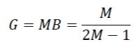
| Voltage gain G is given by | ||||||||||||||||||||||||||
 |
||||||||||||||||||||||||||
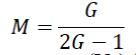
| The maximum modulation index that can be used for any desired voltage gain (G) | ||||||||||||||||||||||||||
 |
||||||||||||||||||||||||||
| is the voltage stress across the switch. The voltage stress (Vs) for simple boost control can be calculated by | ||||||||||||||||||||||||||
| Therefore the voltage stress across the switch for SBC is high, so the obtainable output voltage gain is limited. | ||||||||||||||||||||||||||
| B. Maximum Boost Control (MBC) | ||||||||||||||||||||||||||
| MBC can reduce the voltage stress across the switch and voltage boost can be obtained by turning all traditional zero state into shoot through state. Without distorting output waveform the maximum and B can be obtained for any modulation index. When the triangular signal is either greater than maximum curve of references or lower than minimum of references, shoot through states are generated. In the inductor current and capacitor voltage, low frequency current ripples are introduced. The waveform for maximum boost control is shown in fig: 9. | ||||||||||||||||||||||||||
| The six active states remain unchanged and zero state is turned into shoot through state and thereby without distorting the output waveform the maximum and B can be obtained for any modulation index. | ||||||||||||||||||||||||||
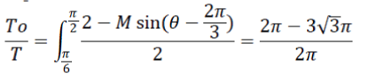
| The maximum boost control can be implemented as in Fig 10. At every ) ST repeats periodically. The switching frequency is assumed to be much higher than modulation frequency. In the interval the average shoot through duty ratio over one switching cycle can be expressed as | ||||||||||||||||||||||||||
 |
||||||||||||||||||||||||||
| Maximum shoot through duty ratio can be expressed as | ||||||||||||||||||||||||||
 |
||||||||||||||||||||||||||
| The shaded portion in fig: 11 indicate the operating region. The output voltage decrease as modulation index increases. Wide operating region is available for MBC when compared with SBC. A high modulation index can be used for a given voltage gain, which implies that the voltage stress across the switch is less. | ||||||||||||||||||||||||||
| To increase the modulation index range third harmonic injection is commonly used in three phase inverter system. This is used here too, to increase the modulation index range thereby to increase the system voltage gain. The maximum modulation index that can be achieved is ) which can be achieved at third harmonic injection. | ||||||||||||||||||||||||||
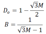
| C. Maximum Constant Boost Control (MCBC) | ||||||||||||||||||||||||||
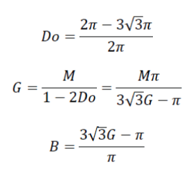
| To reduce the volume and cost, the shoot through duty ratio should be kept constant and greater voltage boost for the given modulation index is required to reduce the voltage stress across the switch [12]. ST duty ratio is required to be kept constant to reduce volume and cost. For a given modulation index, greater voltage boost can be obtained thereby reduce the voltage stress across the switch. There are five modulation curves for this control which include three reference signals and two ST envelope | ||||||||||||||||||||||||||
| When carrier signal is greater than upper envelope signal or less than the lower envelope signal shoot through state is generated. In between the ST state, it operates as traditional PWM control. By keeping ST duty ratio Do constant, maximum boost and voltage gain can be obtained. Therefore current ripples through the inductor can be completely reduced. The inverter can buck or boost the voltage from zero to any desired value within the limit of device voltage. The fig: 13 show the waveform for maximum constant boost control. | ||||||||||||||||||||||||||
 |
||||||||||||||||||||||||||
| The curve for voltage gain verses modulation index is shown in fig 12. From the figure it can be seen that, the voltage gain approaches infinity when modulation index decreases to 3 . The maximum constant boost control can be implemented with third harmonic injection. | ||||||||||||||||||||||||||
RESULTS AND DISCUSSION |
||||||||||||||||||||||||||
| Simulation is performed using MATLAB/SIMULINK software. Simulink library files include inbuilt models of many electrical and electronics components and devices such as diodes, IGBTs, capacitors, inductors, power supply, sine wave generators and so on. The simulation is performed with a resistive and inductive load of 1000Ω and 1000mH. | ||||||||||||||||||||||||||
CONCLUSION |
||||||||||||||||||||||||||
| In this paper, three ST boost control methods are reviewed for a quasi Z source inverter. Critical investigation on various modulation techniques is performed. Proper control method should be selected according to the requirement of different load. The results of various control methods are performed for same input and system parameters. The performance of quasi Z source is better obtained for maximum constant boost control. | ||||||||||||||||||||||||||
|
|
||||||||||||||||||||||||||
Figures at a glance |
||||||||||||||||||||||||||
|
||||||||||||||||||||||||||
References |
||||||||||||||||||||||||||
|


