INTRODUCTION
|
| In embedded systems, data traffic has increased dramatically in recent years. As technology marches forward, simple and high speed interconnect that provides a low cost, unified interconnect, with other different protocols mapped onto it, had become practical. To meet versatile and ever changing I/O needs with these unified interconnect for embedded system, a high speed and highly adaptive IOH (I/O Hub) architecture will provide satisfying flexibility. Some embedded systems provide various IOHs to meet different application requirements, e. g, Intel provides about 20 kinds of Embedded Intel® Architecture chipsets for customers [1]. NXP produce 87 kinds of platforms to support 64 kinds of IOs [2]. Light Peak [4] is a high-bandwidth, inexpensive optical interconnect technology developed by Intel. The protocol itself provides the features very suitable for different applications [5]: |
| • The use of small packet sizes to achieve low latency. |
| • The ability to multiplex multiple I/O protocols over a common link with high bandwidth efficiency. |
| • The ability to allocate link bandwidth using priority and bandwidth reservation mechanisms. |
| On the other hand, FPGA’s native features on flexibility empower it to support different applications. Besides it, latest FPGA adopts advanced transceiver technology to support future communication system. Here, based on FPGA and LPK technology, we present an embedded system IO HUB solution with high bandwidth and multi protocols support. This solution provides unified interface for protocols mapping, replacing numerous individual hardware controller by utilizing LPK’s versatile host controller, thus reduce cost and development efforts for embedded systems, and enhances the IOH flexibility. SATA, Ethernet and Display Port are implemented on the platform. |
| Benchmarks’ result shows performance of each protocol is competitive with the native one. The platform is implemented on Xilinx FPGA V5 series plus 10Gbps x2 optical PHY modules. And we map SATA, Display Port and Ethernet on it. |
SYSTEM ARCHITECTURE
|
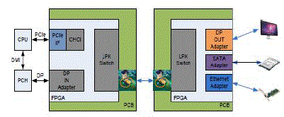
| The platform consists of the host computer, FPGA board and the end device as Fig. 1 shows. The board consists of aFPGA module, LPK optical modules and several connectors such as SATA, Display and Ethernet. In host side, FPGA can either attach on PCIe bus to access the data from the main memory, or it can attach to the native hardware controller, such as Display Port, to receive data, as Fig. 1 shows. In device side, FPGA attach the end device and transfer the data of end device on fiber. |
| When application transfer data on a certain protocol via the proposed optical IOH, the host computer may has the hardware controller of the native protocol, or it may not. In first case, i.e. DisplayPort, the protocol data received by the FPGA is real packet flow generated by the native hardware controller in host computer. Hardware IN adaptor in FPGA reorganizes the packets and encapsulates the data into LPK packet. Then the LPK hardware processes the packets and sends out the packets through the fiber. In the second case, i.e. SATA and Ethernet, we provide a soft stack framework which takes the place of the native hardware controller. The software stack directly organizes protocol format data as LPK required, and then the CHCI fetch the data to the LPK low layer hardware to finally send it out in LPK packets. In the device side, the LPK packets are received by the FPGA and converted back to the native protocol format. The switch dispatches the data to the corresponding hardware protocol engine, which unpack the protocol format header and data and finally transfer it to the end device. |
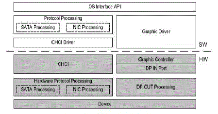
| Fig. 2 shows the platform architecture stack, which consists of: |
| • A software interface that binds with Operating System (OS). OS defines standard interface API that needs to be implemented for a class of devices. |
| • A software protocol processing layer which maintains certain protocol states and converts OS primitives to semantics that is predefined in product design. The layer extracts a uniform interface to OS block device layer, which is a great relief to low level driver developers. |
| • A CHCI interfacing layer that manages the actual data transfer between host memory and underlying hardware. |
| • A hardware CHCI interface layer, providing hardware queue processing, DMA operations etc.• A hardware protocol processing layer normally contains transaction tracking, data interfacing and host data to device protocol data unit conversion. The detail design and working flow will be introduced in the following sections. |
HARDWARE ARCHITECTURE
|
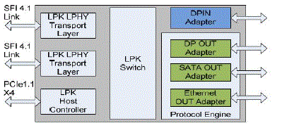
| The hardware platform can be configured as the host side equipment or the device side equipment. In host side configuration, all the native protocol packets are converted into LPK packets via LPK host controller or IN adapters; in device side configuration, all the LPK packets received from optical link are transformed back into native protocol packets and dispatched to corresponding OUT adapters.The platform consists of two major parts: the optical module and the FPGA. The optical module provides a high bandwidth PHY layer up to 10Gbps, and converts electrical signals from the 10Gig transceiver into optical pulses to feed into connectors [6]. The FPGA is designed to provide the following components, shown in Fig. 3: |
| • LPK logical PHY and transport layer: LPK link training, clock difference compensation, packet verification and classification. |
| • LPK switch: dispatch each LPK packet to destination. Provide flow control and QoS scheduling based on the information in packet header. |
| • LPK host controller (CHCI): LPK Host controller is defined for exchanging frames between the host memory and the LPK fabric in FPGA. The DMA engine in it moves data with high efficiency and low latency through standard PCIe transactions. In the TX direction, frames from the host memory are segmented into LPK packets and then forwarded via LPK network. In the RX direction, LPK packets are reassembled to form a frame needed by the software and uploaded to the host memory by the DMA engine. |
| • IN adapter: encapsulating native protocol packets and data stream into LPK packets. |
| • Protocol engine: universal protocol engine which can be customized into various kinds of OUT adapters to meet different interface protocols’ requirements such as DisplayPort, SATA, Ethernet and so on. We present the detail design of protocol engine below. |
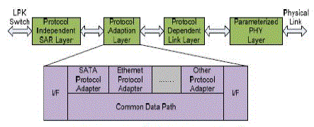
| Fig. 4 shows the detailed architecture of protocol engine. |
| In our design, it consists of four layers: Protocol independent SAR (Segmentation & reassembly) layer, protocol adaption layer, protocol dependent link layer and the PHY layer. |
| • Protocol Independent SAR Layer |
| This layer functions on packets segmentation and reassembly (SAR). Maximum payload size of LPK protocol packet is 256 bytes, far below many native protocols. The native packet needs to be processed before it is transferred on the LPK fiber. Segmentation refers to the process of creating multiple LPK packets from a single frame and reassembly refers to the process of creating a single frame from multiple LPK packets in the opposite direction. |
| • Protocol Adaption Layer |
| This layer implements protocol translation between LPK and native protocols. Protocol adaption layer will classify the packets into two types according to information in LPK packet header: data packets and protocol packets. Data packets will be forwarded to Link layer directly. Protocol packets will be terminated or used to control the link layer as what the native protocol required. For example, the packet is a MDIO packet from the host side which is used to read the current Ethernet link status, the protocol adaption layer will terminate this packet, read corresponding link status registers and prepare the reply packet in Ethernet required format, then it will propose a request to SAR layer with the reply packet as LPK payload and indicate packet type as MDIO in LPK packet header. |
| As mentioned above, user can configure this layer to support different native protocols, only protocol part is different, |
| data path and adjacent layer interface are the same. • Protocol Dependent Link layer Each protocol has its own link training flow, here we use discrete state machine for each protocol. In the future, we consider merging the common part to one state machine. • Parameterized PHY Layer |
| We directly configure the FPGA embedded transceiver for different native protocol PHY. We set a lot of parameters in transceiver configuration such as link speed, encoding method, COMMA sets, channel bonding, electrical characteristics, etc. |
SOFTWARE ARCHITECTURE
|
| The original LPK hardware solution maps the I/O protocol with pairs of IN and OUT LPK adapters. It requires no changes to the current kernels. The IN adapter in the IN port connects the native hardware controller to the LPK switch, and the OUT adapter of the OUT port connects the device to the LPK switch. This mechanism does not need extra software work, yet it need the system support many different native protocol hardware controller. |
| Here we present a new solution maps the I/O protocol without the native hardware controller and IN adapter. As Fig. 4 shows, this solution moves the host side protocol processing logics from hardware to software. The software architecture is designed as follows: |
| • OS Interface API – The OS kernel defines standard interface API the needs to be implemented for a class of devices. |
| • Protocol processing layer – maintains the protocol states and converts upper layer primitives to semantics that used to appear in the native hardware controllers. |
| • CHCI interface software – manages the data transfer between host memory and underlying hardware, reports transfer completion and provide common protocol processing functions to the protocol processing layer. We have successfully mapped SATA and NIC protocols with this solution. CHCI driver, SATA driver and NIC driver are implemented in Linux 2.6.25 to support the mapping. Other upper layers such as SCSI, Block, Core network, VFS layer are left untouched. |
ERFORMANCE
|
| We do several experiments to measure the overhead of the architecture. We run SATA and NIC respectively under the Native environment and our platform environment. Here “Native” refers to the environment where data transfer on its original protocol connection. |
| A. SATA Testing Setup and Performance |
| We have deployed IO meter to test the SATA disks. To analyze our architecture impacts on SATA’s performance, we have let the clients perform read/write disk operations with different block sizes in both environments, and collected throughput and CPU utilization data. |
| Fig. 5.(a) and Fig. 5.(b) respectively show the SATA’s read/write performance in both the Native environment and our environment. The throughput of the read/write on our platform is very close to that of the Native’s. It’s worth noting that our read throughput is relatively a bit higher. The reason is because there’s a memory copy in the packet reception of our SATA driver, leading to more cache hits and a higher throughput, but pays for a higher CPU utilization. B. NIC Testing Setup and Performance |
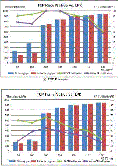
| We have deployed testing tool Iperf to test NICs. In the Native environment, the client and the server are connected directly with a network cable while in ours they are connected through the LPK fabric across optical fiber. To analyze our architecture impacts on NIC’s performance in our experiment, we have let the clients perform TCP transmission/reception operations with different MSS (Maximum Segment Size), and collected the throughput and the CPU utilization. |
| Fig. 6.(a) and Fig. 6.(b) show the NIC’s TCP reception/transmission performance in both the Native environment and our environment. The throughput of the LPK is very close to the native’s. But there are some divergences we need to explain. Look at Fig. 6.(a), our throughput at 50, 100 bytes are much higher. It’s due to that our NIC driver doesn’t implement the dynamic algorithm of controlling interruption rate which is implemented in the NIC driver of the native environment. So the interrupt rates of NICs in two environments are different. And higher interrupt rate of our environment leads to lower latency in TCP transactions, but pays for higher CPU utilization. The similar thing happens in Fig. 6.(b). |
| C. Conclusion |
| From these testing, we see that our proposed architecture brings some overhead as we expected, yet it is very small. By further optimizing our software and hardware implementation, we can achieve smaller overhead. |
SUMMARY
|
| In this paper, we present an embedded system IO HUB solution with high bandwidth and multi-protocol support based on FPGA and LPK technology. The solution considers various connect environments with or without native device controller and covers both host side and device side, and covers the system. We present a software stack framework that provides a unified interface for protocols mapping, replacing numerous native hardware controller, by utilizing LPK’s versatile host controller, thus reduce cost and development efforts, and enhance the IOH flexibility. SATA, Ethernet and Display are implemented on the platform. Benchmarks’ result show performance of each protocol is competitive with the native one. |
Figures at a glance
|
 |
 |
 |
| Figure 1 |
Figure 2 |
Figure 3 |
 |
 |
 |
| Figure 4 |
Figure 5 |
Figure 6 |
|
| |
References
|
- Robert A. Burckle, “SUMIT I/O Expansion Guides Next- Generation Intel® Processors into Express Lanes”,WinSystemsInc
- Intel, “embedded IO survey” not published, 2010.
- LSI, “Fusion-MPT™ Architecture”, 2007.
- http://www.intel.com/go/lightpeak/index.htm.
- SreenivasAddagatla, et al. "Direct Network Prototype Leveraging Light Peak Technology," hoti, pp.109 112, 2010, 18th IEEE Symposium on
|